A3969 Ver la hoja de datos (PDF) - Allegro MicroSystems
Número de pieza
componentes Descripción
Fabricante
A3969 Datasheet PDF : 9 Pages
| |||
A3969
Dual Full-Bridge PWM Motor Driver
FUNCTIONAL DESCRIPTION
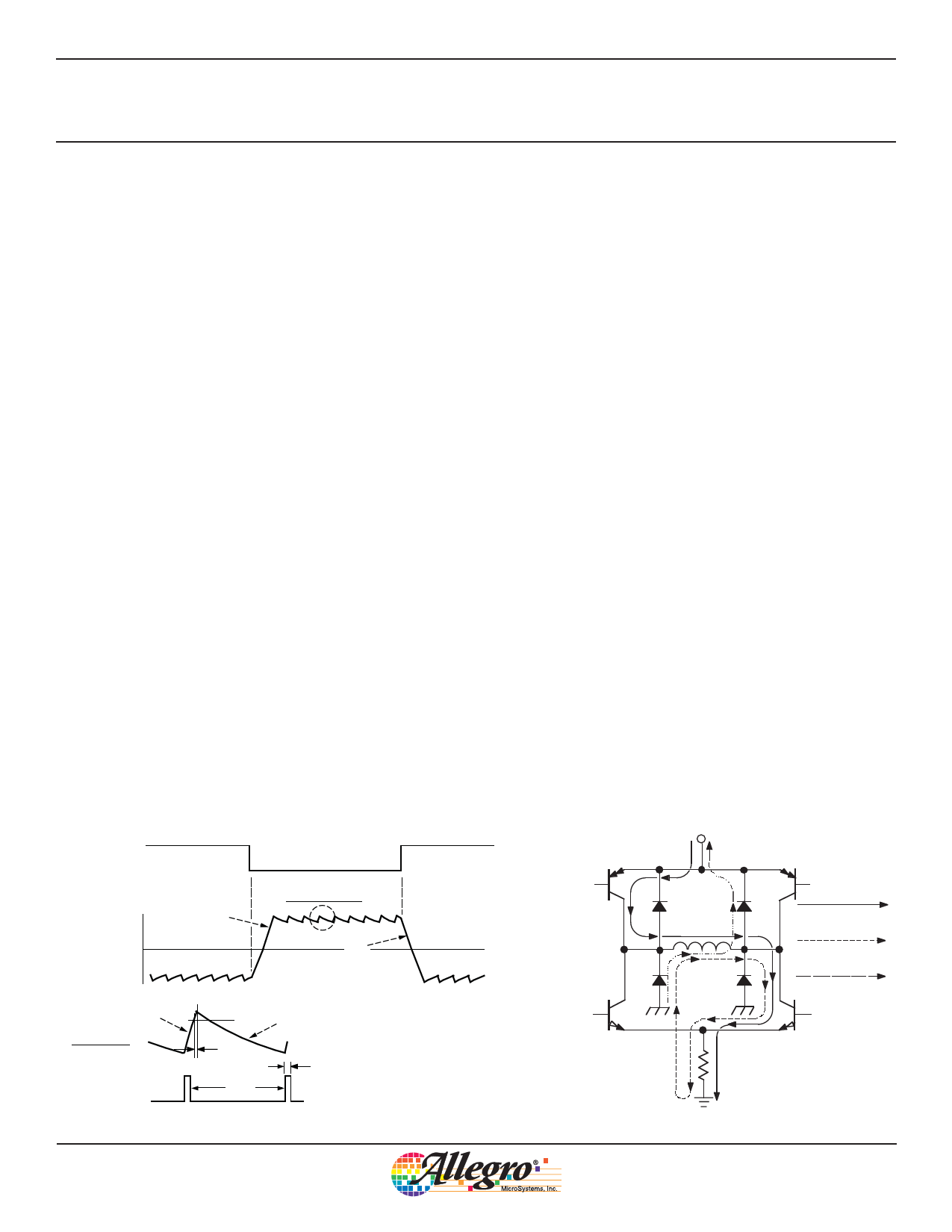
Internal PWM Current Control. The A3969 dual
H-bridge is designed to drive both windings of a bipolar
stepper motor. Load current can be controlled in each mo-
tor winding by an internal fixed-frequency PWM control
circuit. The current-control circuitry works as follows:
when the outputs of the H-bridge are turned on, current in-
creases in the motor winding. The load current is sensed by
the current-control comparator via an external sense resis-
tor (RS). Load current continues to increase until it reaches
the predetermined value, set by the selection of external
current-sensing resistors and reference input voltage (VREF)
according to the equation:
ITRIP = IOUT + ISO = VREF/(4 RS)
where ISO is the sense-current error (typically 18 mA) due
to the base-drive current of the sink driver transistor.
At the trip point, the comparator resets the source-en-
able latch, turning off the source driver of that H-bridge.
The source turn off of one H-bridge is independent of the
other H-bridge. Load inductance causes the current to
recirculate through the sink driver and ground-clamp diode.
The current decreases until the internal clock oscillator sets
the source-enable latches of both H-bridges, turning on
the source drivers of both bridges. Load current increases
again, and the cycle is repeated.
The frequency of the internal clock oscillator is set by
the external timing components RTCT. The frequency can
be approximately calculated as:
fosc = 1/(RT CT + tblank)
where tblank is defined below.
The range of recommended values for RT and CT are
20 k to 100 k and 470 pF to 1000 pF respectively.
Nominal values of 56 k and 680 pF result in a clock
frequency of 25 kHz.
Current-Sense Comparator Blanking. When the
source driver is turned on, a current spike occurs due to
the reverse-recovery currents of the clamp diodes and
switching transients related to distributed capacitance in
the load. To prevent this current spike from erroneously
resetting the source enable latch, the current-control com-
parator output is blanked for a short period of time when
the source driver is turned on. The blanking time is set by
the timing component CT according to the equation:
tblank = 1900 CT (μs).
A nominal CT value of 680 pF will give a blanking
time of 1.3 μs.
The current-control comparator is also blanked when
the H-bridge outputs are switched by the PHASE or EN-
ABLE inputs. This internally generated blank time is
approximately 1 μs.
V PHASE
+
I OUT 0
–
BRIDGE
ON
See Enlargement A
ALL
OFF
BRIDGE
ON
Enlargement A
INTERNAL
OSCILLATOR
ITRIP
td
RTCT
SOURCE
OFF
tblank
Dwg. WM-003-2
V
BB
BRIDGE ON
SOURCE OFF
ALL OFF
RS
Dwg. EP-006-16
Allegro MicroSystems, Inc.
6
115 Northeast Cutoff, Box 15036
Worcester, Massachusetts 01615-0036 (508) 853-5000
www.allegromicro.com
Share Link: 