A3969 Ver la hoja de datos (PDF) - Allegro MicroSystems
Número de pieza
componentes Descripción
Fabricante
A3969 Datasheet PDF : 9 Pages
| |||
A3969
Dual Full-Bridge PWM Motor Driver
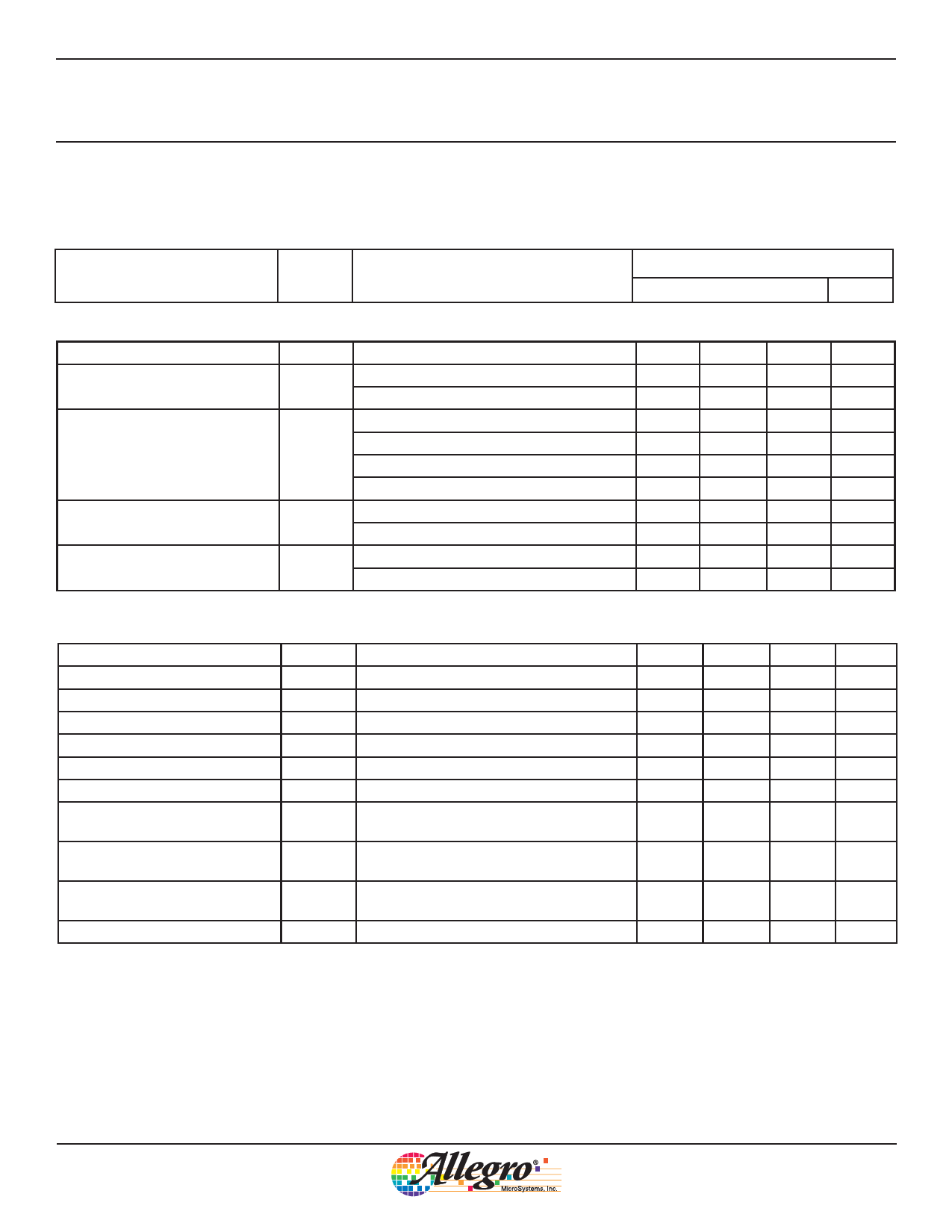
ELECTRICAL CHARACTERISTICS at TA = +25°C, VBB = 30 V, VCC = 3.0 V to 3.6 V, VREF = 1.7 V,
VS = 0 V, 56 kΩ and 680 pF RC to Ground (unless noted otherwise)
Characteristic
Symbol Test Conditions
Min.
Limits
Typ. Max.
Units
Output Drivers
Load Supply Voltage Range
VBB Operating, IOUT = ±650 mA, L = 3 mH
5
—
30
V
Output Leakage Current
ICEX
VOUT = 30 V
VOUT = 0 V
—
<1.0
50
μA
—
<-1.0
-50
μA
Source Driver, IOUT = -400 mA
—
1.7
2.0
V
Output Saturation Voltage
VCE(SAT)
Source Driver, IOUT = -650 mA
Sink Driver, IOUT = +400 mA, VS = 0.425 V
—
—
1.8
2.1
0.3
0.5
V
V
Sink Driver, IOUT = +650 mA, VS = 0.425 V
—
0.7
1.3
V
Clamp Diode Forward Voltage
VF
IF = 400 mA
IF = 650 mA
—
1.1
1.4
V
—
1.4
1.6
V
Motor Supply Current
(No Load)
IBB(ON)
IBB(OFF)
VENABLE1 = VENABLE2 = 0.8 V
VENABLE1 = VENABLE2 = 2.4 V
—
3.0
5.0
mA
—
<1.0
200
μA
Control Logic
Logic Supply Voltage Range
Logic Input Voltage
Logic Input Current
Reference Input Volt. Range
Reference Input Current
Reference Divider Ratio
Current-Sense Comparator
Input Offset Voltage
Current-Sense Comparator
Input Voltage Range
Sense-Current Offset
VCC
VIN(1)
VIN(0)
IIN(1)
IIN(0)
VREF
IREF
VREF/
VTRIP
VIO
Operating
VIN = 2.4 V
VIN = 0.8 V
Operating
VREF = 0 V
VS
Operating
ISO
IS – IOUT, 50 mA ≤ IOUT ≤ 650 mA
NOTES:
1. Typical Data is for design information only.
2. Negative current is defined as coming out of (sourcing) the specified device terminal.
3.00
—
3.60
V
2.4
—
—
V
—
—
0.8
V
—
<1.0
20
μA
—
<-20
-200
μA
0.1
–
1.7
V
-2.5
0
1.0
μA
3.8
4.0
4.2
—
-6.0
0
6.0
mV
-0.3
—
0.425
V
12
18
24
mA
Allegro MicroSystems, Inc.
4
115 Northeast Cutoff, Box 15036
Worcester, Massachusetts 01615-0036 (508) 853-5000
www.allegromicro.com
Share Link: 