A2557 Ver la hoja de datos (PDF) - Allegro MicroSystems
Número de pieza
componentes Descripción
Fabricante
A2557 Datasheet PDF : 12 Pages
| |||
2557
PROTECTED QUAD DRIVER
WITH FAULT DETECTION
& SLEEP MODE
CIRCUIT DESCRIPTION AND APPLICATION (continued)
IN
FAULT
(SHORTED
LOAD)
FAULT
(OPEN
LOAD)
WITH OUTPUT CAPACITOR
Dwg. WP-035
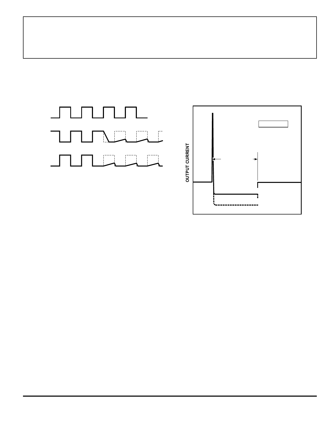
Under some conditions it is possible to get spurious
glitches on the FAULT output at load turn-on and turn-off
transitions:
• Light load turn-off. Under light loading conditions the
turn-off delay (see characteristics above) of the output stage
increases and may result in a spurious fault output of a few µs
(the duration being proportional to the turn-off delay). As it is
difficult to define this over all operating conditions, if a
particular application would be sensitive to this type of glitch,
then it is generally recommended to include a small (about
0.01 µF) smoothing/storage capacitor at the FAULT output.
• Incandescent lamp turn-on. As described above, driving an
incandescent filament results in the driver operating in current
limit for a period after turn-on. During this period a “fault”
condition will be indicated (over current). As discussed above
this period can be 10s of ms. To avoid this indication, the
capacitor on the FAULT output would need to be increased to
provide an appropriate time constant. Alternatively, in a
microcontroller-based system, the code could be written to
ignore the FAULT condition for an appropriate period after
lamp turn on.
Correct FAULT operation cannot be guaranteed with an
unconnected output — unused outputs should not be turned on,
or unused outputs should be pulled high to >2.5 V, and/or
associated inputs tied low.
NOT TO SCALE
SHORT CIRCUIT
NORMAL LOAD
CURRENT LIMIT (12 V SUPPLY)
CURRENT LIMIT (24 V SUPPLY)
TIME
Thermal considerations
Dwg. WP-013-1
Device power dissipation can be calculated as:
PD = (VO1 x IO1 x duty cycle1) + … + (VO4 x IO4 x duty cycle4)
+ (VCC x ICC)
Note - ICC is also modulated by the duty cycle, but this is a
reasonable approximation for most purposes.
This can then be compared against the permitted package
power dissipation, using:
Permitted PD = (150 – TA)/RθJA
where RθJA is given as:
28-lead PLCC (part number suffix ‘–EB’) = 36°C/W
16-pin PDIP (part number suffix ‘–B’) = 43°C/W
16-lead SOIC (part number suffix ‘–LB’) = 90°C/W
RθJA is measured on typical two-sided PCB. Additional
information is available on the Allegro web site.
www.allegromicro.com
8
Share Link: 