A2557 Ver la hoja de datos (PDF) - Allegro MicroSystems
Número de pieza
componentes Descripción
Fabricante
A2557 Datasheet PDF : 12 Pages
| |||
2557
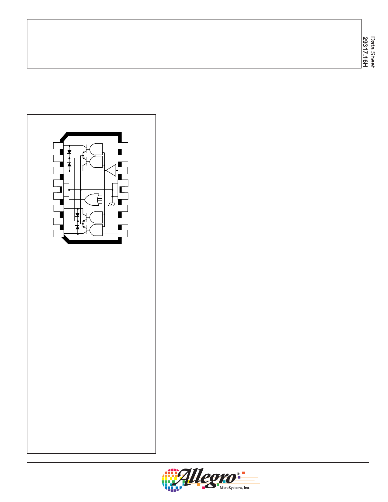
PROTECTED QUAD LOW-SIDE DRIVER
WITH FAULT DETECTION and SLEEP MODE
A2557xLB (SOIC)
OUT 1 1
K2
OUT 2 3
GROUND 4
GROUND 5
OUT 3 6
FAULT 7
OUT 4 8
16 IN 1
15 IN 2
14 ENABLE
13 GROUND
12 GROUND
11 V CC
10 IN 3
9 IN 4
Dwg. PP-017-4
Note that the A2557xB (DIP) and the A2557xLB
(SOIC) are electrically identical and share a
common terminal number assignment.
ABSOLUTE MAXIMUM RATINGS
Output Voltage, VO .............................. 60 V
Over-Current Protected Output Voltage,
VO ..................................................... 32 V
Output Current, IO ......................... 500 mA*
FAULT Output Voltage, VFLT ............. 60 V
Logic Supply Voltage, VCC ................. 7.0 V
Input Voltage, VI or VOE ..................... 7.0 V
Package Power Dissipation,
PD ........................................... See Graph
Operating Temperature Range, TA
Suffix ‘S-’ ...................... -20°C to +85°C
Suffix ‘E-’ ...................... -40°C to +85°C
Suffix ‘K-’ ................... -40°C to +125°C
Junction Temperature,
TJ ............................................... +150°C*
Storage Temperature Range,
TS ................................. -55°C to +150°C
*Outputs are current limited at approximately
500 mA per driver and junction temperature
limited if higher current is attempted.
The A2557xB, A2557xEB, and A2557xLB have been specifically
designed to provide cost-effective solutions to relay-driving applications with
up to 300 mA drive current per channel. They may also be used for driving
incandescent lamps in applications where turn-on time is not a concern. Each
of the four outputs will sink 300 mA in the on state. The outputs have a
minimum breakdown voltage of 60 V and a sustaining voltage of 40 V. A
low-power Sleep Mode is activated with either ENABLE low or all inputs
low. In this mode, the supply current drops to below 100 µA.
Over-current protection for each channel has been designed into these
devices and is activated at a nominal 500 mA. It protects each output from
short circuits with supply voltages up to 32 V. When an output experiences a
short circuit, the output current is limited at the 500 mA current clamp. In
addition, foldback circuitry decreases the current limit if an excessive voltage
is present across the output and assists in keeping the device within its SOA
(safe operating area). An exclusive-OR circuit compares the input and output
state of each driver. If either a short or open load condition is detected, a
single FAULT output is turned on (active low).
Continuous or multiple overload conditions causing the channel tempera-
ture to reach approximately 165°C will result in an additional linear decrease
in the output current of the affected driver. If the fault condition is corrected,
the output stage will return to its normal saturated condition.
The packages offer fused leads for enhanced thermal dissipation. Package
B is 16-pin power DIP with exposed tabs, EB is 28-lead power PLCCs, and
LB are 16-lead power wide-body SOICs for surface-mount applications. The
lead (Pb) free versions have 100% matte tin leadframe plating.
FEATURES
■ 300 mA Output Current per Channel
■ Independent Over-Current Protection &Thermal Limiting for Each Driver
■ Output Voltage to 60 V
■ Output SOA Protection
■ Fault-Detection Circuitry for Open or Shorted Load
■ Low Quiescent Current Sleep Mode
■ Integral Output Flyback/Clamp Diodes
■ TTL- and 5 V CMOS-Compatible Inputs
Share Link: 