74LVC273D Ver la hoja de datos (PDF) - Philips Electronics
Número de pieza
componentes Descripción
Fabricante
74LVC273D Datasheet PDF : 10 Pages
| |||
Philips Semiconductors
Octal D-type flip-flop with reset; positive-edge trigger
Product specification
74LVC273
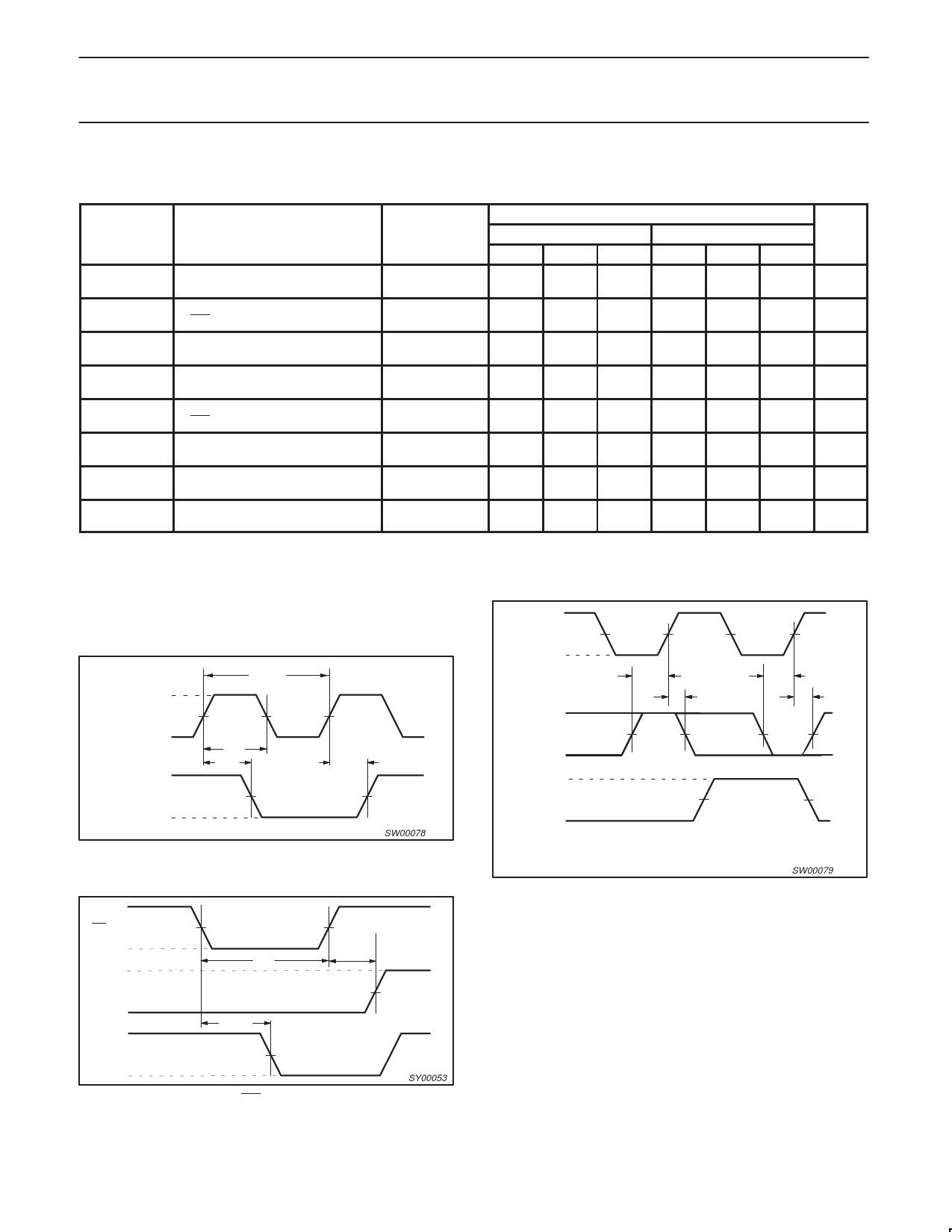
AC CHARACTERISTICS
GND = 0V; tR = tF = 2.5ns; CL = 50pF; RL = 500Ω; Tamb = –40°C to +85°C.
SYMBOL
PARAMETER
WAVEFORM
tPHL
Propagation delay
tPLH
CP to Qn
1
tPHL
Propagation delay
MR to Qn
2
tW
Clock pulse width
HIGH or LOW
1
tW
Master reset pulse
width LOW
2
trem
Removal time
MR to CP
2
tsu
Set-up time
Dn to CP
3
th
Hold time
Dn to CP
3
fmax
Maximum clock
pulse frequency
1
NOTE:
1. These typical values are at VCC = 3.3V and Tamb = 25°C.
LIMITS
VCC = 3.3V ±0.3V
MIN TYP1 MAX
VCC = 2.7V
MIN TYP MAX
6.0
10.2
6.6
11.2
6.3
11.0
7.4
12.0
4
1.2
5
1.8
4
1.2
5
1.7
2
–1.0
3
–1.0
2
0.7
3
1.0
0
–0.6
0
–0.9
125
100
UNIT
ns
ns
ns
ns
ns
ns
ns
MHz
AC WAVEFORMS
VM = 1.5V at VCC w 2.7V.
VM = 0.5 VCC at VCC t 2.7V.
VOL and VOH are the typical output voltage drop that occur with the
output load.
1/fMAX
VI
CP INPUT
GND
VOH
VM
tw
tPHL
tPLH
Qn OUTPUT
VM
VOL
SW00078
Waveform 1. Clock (CP) to output (Qn) propagation delays, the
clock pulse width and the maximum clock pulse frequency
VCC
MR INPUT
VM
VM
GND
VCC
CP INPUT
GND
VOH
tw
tPHL
trem
VM
Qn OUTPUT
VOL
VM
SY00053
Waveform 2. Master reset (MR) pulse width, the master reset to
output (Qn) propagation delays and the master reset to clock
(CP) removal time
VI
CP
INPUT
VM
GND
tsu
tsu
ÉÉÉÉ VI
Dn
ÉÉÉÉ INPUT
VM
ÉÉÉÉ GND
ÉÉÉth ÉÉÉÉÉÉÉÉÉÉÉÉÉÉÉth ÉÉÉ
VOH
Qn
OUTPUT
VM
VOL
NOTE: The shaded areas indicate when the input is permitted to change
for predictable output performance.
SW00079
Waveform 3. Data set-up and hold times for the data input (Dn)
1998 May 20
5
Share Link: 