74LVC273PW Ver la hoja de datos (PDF) - Philips Electronics
Número de pieza
componentes Descripción
Fabricante
74LVC273PW Datasheet PDF : 10 Pages
| |||

Philips Semiconductors
Octal D-type flip-flop with reset; positive-edge trigger
Product specification
74LVC273
FEATURES
• Wide supply voltage range of 1.2V to 3.6V
• Conforms to JEDEC standard 8-1A
• Inputs accept voltages up to 5.5V
• CMOS low power consumption
• Direct interface with TTL levels
• Output drive capability 50Ω transmission lines @ 85°C
DESCRIPTION
The 74LVC273 is a low-voltage Si-gate CMOS device, superior to
most advanced CMOS compatible TTL families.
The 74LVC273 has eight edge-triggered , D-type flip-flops with
individual D inputs and Q outputs. The common clock (CP) and
master reset (MR) inputs load and reset (clear) all flip-flops
simultaneously. The state of each D input, one set-up time before
the LOW-to-HIGH clock transition, is transferred to the
corresponding output (Qn) of the flip-flop.
All outputs will be forced LOW independently of clock or data inputs
by a LOW voltage level on the MR input.
The device is useful for applications where the true output only is
required and the clock and master reset are common to all storage
elements.
QUICK REFERENCE DATA
GND = 0V; Tamb = 25°C; tr =tf v2.5 ns
SYMBOL
PARAMETER
CONDITIONS
tPHL/tPLH
Propagation delay
CP to Qn;
MR to Qn
CL = 50pF
VCC = 3.3V
fmax
Maximum clock frequency
CI
Input capacitance
CPD
Power dissipation
capacitance per flip-flop
VI = GND to VCC1
NOTE:
1 CPD is used to determine the dynamic power dissipation (PD in µW)
PD = CPD VCC2 x fi )S (CL VCC2 fo) where:
fi = input frequency in MHz; CL = output load capacity in pF;
fo = output frequency in MHz; VCC = supply voltage in V;
S (CL VCC2 fo) = sum of the outputs.
TYPICAL
6.0
6.0
230
5.0
22
ORDERING INFORMATION
PACKAGES
20-Pin Plastic SO
20-Pin Plastic SSOP Type II
20-Pin Plastic TSSOP Type I
TEMPERATURE RANGE
–40°C to +85°C
–40°C to +85°C
–40°C to +85°C
OUTSIDE NORTH AMERICA
74LVC273 D
74LVC273 DB
74LVC273 PW
NORTH AMERICA
74LVC273 D
74LVC273 DB
74LVC273PW DH
UNIT
ns
MHz
pF
pF
DWG NUMBER
SOT163-1
SOT339-1
SOT360-1
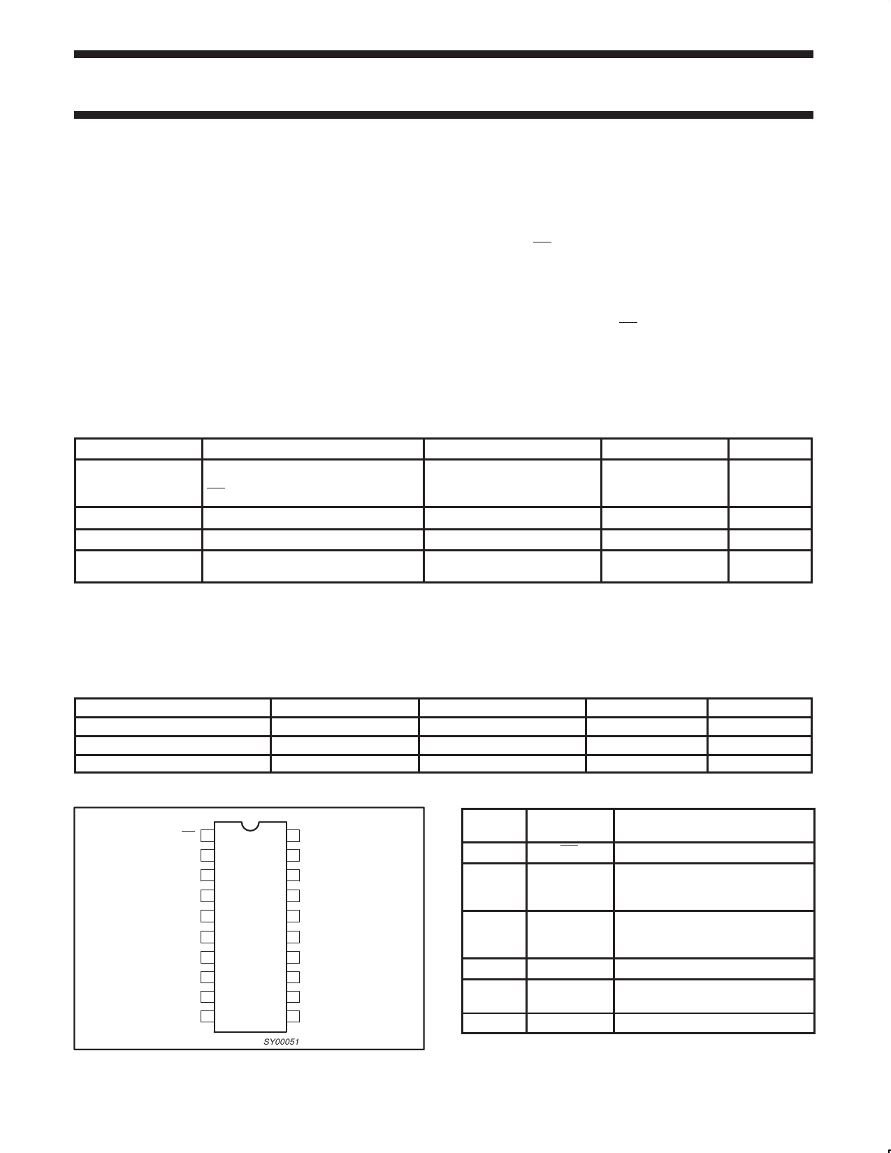
PIN CONFIGURATION
MR 1
Q0 2
D0 3
D1 4
Q1 5
Q2 6
D2 7
D3 8
Q3 9
GND 10
20 VCC
19 Q7
18 D7
17 D6
16 Q6
15 Q5
14 D5
13 D4
12 Q4
11 CP
SY00051
PIN DESCRIPTION
PIN
NUMBER
SYMBOL
1
MR
2, 5, 6,
9, 12, 15,
16, 19
Q0 – Q7
3, 4, 7,
8, 13, 14,
17, 18
D0 – D7
10
GND
11
CP
20
VCC
FUNCTION
Master reset input (active LOW)
Flip-flop outputs
Data inputs
Ground (0V)
Clock input (LOW-to-HIGH,
edge-triggered)
Positive power supply
1998 May 20
2
853-2064 19419