74HCT253DB(2016) Ver la hoja de datos (PDF) - NXP Semiconductors.
Número de pieza
componentes Descripción
Fabricante
74HCT253DB Datasheet PDF : 16 Pages
| |||
Nexperia
74HC253; 74HCT253
Dual 4-input multiplexer; 3-state
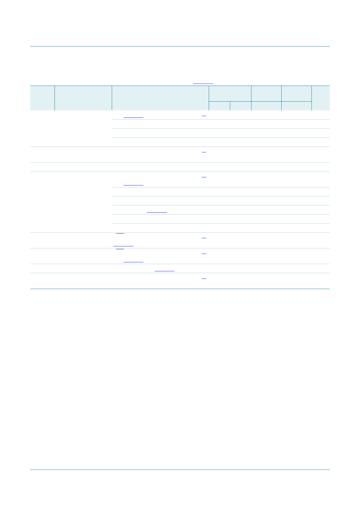
Table 7. Dynamic characteristics …continued
Voltages are referenced to GND (ground = 0 V); For test circuit see Figure 8.
Symbol Parameter
Conditions
25 C
Typ Max
tdis
disable time
nOE to nY; VCC = 4.5 V; [3] 13
30
see Figure 7
tt
transition time VCC = 4.5 V; see Figure 6
5
12
CPD
power dissipation per multiplexer;
[5] 55
-
capacitance
VI = GND to VCC 1.5 V
40 C to +85 C 40 C to +125 C Unit
Max
Max
38
45
ns
15
18
ns
-
-
pF
[1] tpd is the same as tPHL, tPLH.
[2] ten is the same as tPZH, tPZL.
[3] tdis is the same as tPHZ, tPLZ.
[4] tt is the same as tTHL, tTLH.
[5] CPD is used to determine the dynamic power dissipation (PD in W).
PD = CPD VCC2 fi N + (CL VCC2 fo) where:
fi = input frequency in MHz;
fo = output frequency in MHz;
CL = output load capacitance in pF;
VCC = supply voltage in V;
N = number of inputs switching;
(CL VCC2 fo) = sum of outputs.
12. Waveforms
9,
6Q,QOQLQSXW
*1'
92+
Q<RXWSXW
92/
90
90
W3+/
90
W7+/
90
W3/+
W7/+
DDO
Fig 6.
Measurement points are given in Table 8.
VOL and VOH are typical voltage output levels that occur with the output load.
Propagation delays input (Sn, 1In, 2In) to output (nY) and output (nY) transition times
74HC_HCT253
Product data sheet
All information provided in this document is subject to legal disclaimers.
Rev. 6 — 1 February 2016
.
8 of 16
© Nexperia B.V. 2017. All rights reserved
Share Link: 