74ACT715 Ver la hoja de datos (PDF) - Fairchild Semiconductor
Número de pieza
componentes Descripción
Fabricante
74ACT715 Datasheet PDF : 14 Pages
| |||
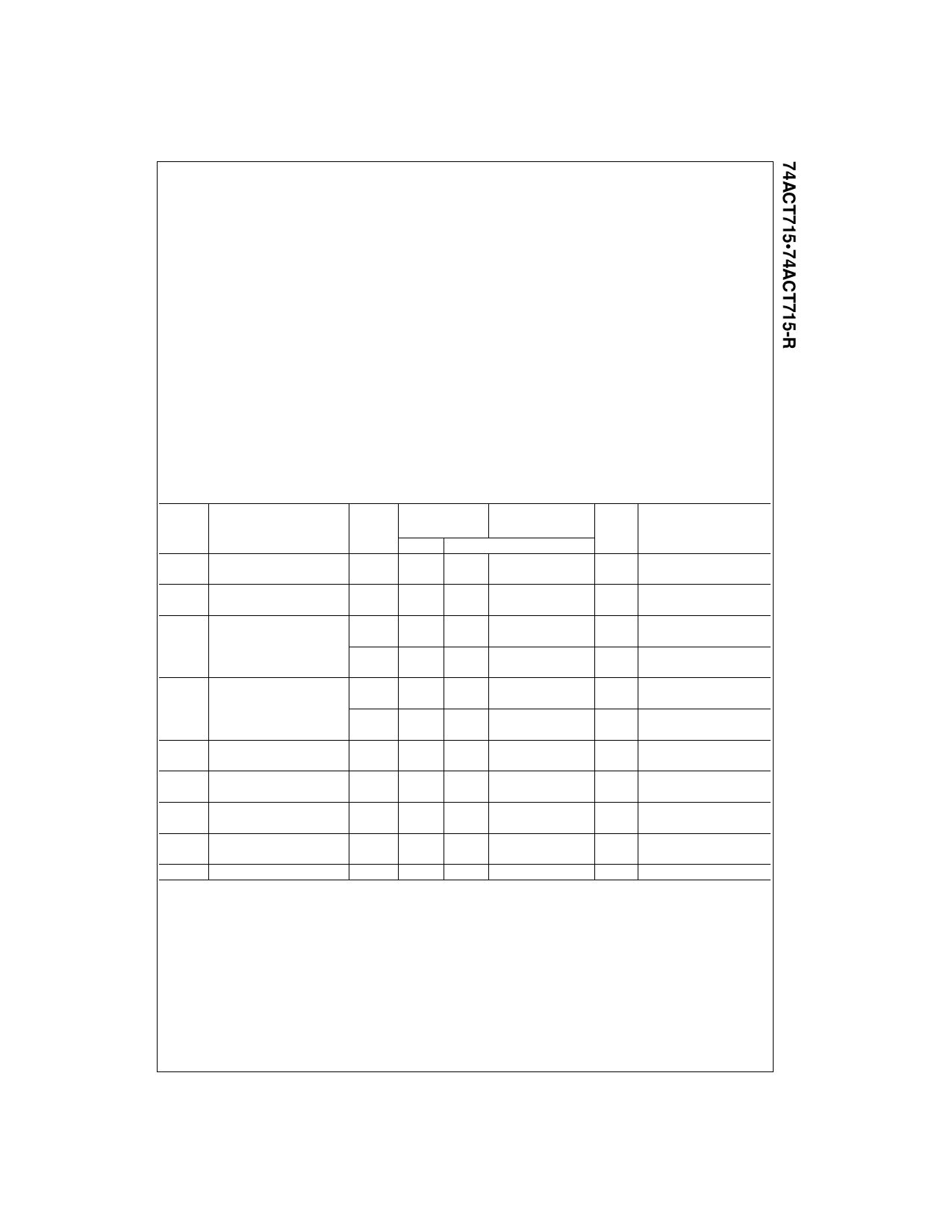
Absolute Maximum Ratings(Note 1)
Supply Voltage (VCC)
DC Input Diode Current (IIK)
VI = −0.5V
VI = VCC +0.5V
DC Input Voltage (VI)
DC Output Diode Current (IOK)
VO = −0.5V
VO = VCC +0.5V
DC Output Voltage (VO)
DC Output Source
or Sink Current (I O)
DC VCC or Ground Current
per Output Pin (I CC or IGND)
Storage Temperature (TSTG)
−0.5V to +7.0V
−20 mA
+20 mA
−0.5V to V CC +0.5V
−20 mA
+20 mA
−0.5V to V CC +0.5V
±15 mA
±20 mA
−65°C to +150°C
Junction Temperature (TJ)
PDIP
140°C
Recommended Operating
Conditions
Supply Voltage (VCC)
Input Voltage (VI)
Output Voltage (VO)
Operating Temperature (TA)
Minimum Input Edge Rate (∆V/∆t)
4.5V to 5.5V
0V to VCC
0V to VCC
−40°C to +85°C
VIN from 0.8V to 2.0V
VCC @ 4.5V, 5.5V
125 mV/ns
Note 1: Absolute maximum ratings are those values beyond which damage
to the device may occur. The databook specifications should be met, with-
out exception, to ensure that the system design is reliable over its power
supply, temperature and output/input loading variables. Fairchild does not
recommend operation of FACT™ circuits outside databook specifications.
DC Electrical Characteristics
For ACT Family Devices over Operating Temperature Range (unless otherwise specified)
TA = +25°C
Symbol
Parameter
VCC
CL = 50 pF
TA = −40°C to +85°C
(V)
Typ
Guaranteed Limits
VIH
Minimum HIGH Level
Input Voltage
4.5
1.5
2.0
2.0
5.5
1.5
2.0
2.0
VIL
Maximum LOW Level
Input Voltage
4.5
1.5
0.8
0.8
5.5
1.5
0.8
0.8
VOH
Minimum HIGH Level
Output Voltage
4.5
4.49
4.4
4.4
5.5
5.49
5.4
5.4
4.5
3.86
3.76
5.5
4.86
4.76
VOL
Maximum LOW Level
Output Voltage
4.5
0.001
0.1
0.1
5.5
0.001
0.1
0.1
4.5
0.36
0.44
5.5
0.36
0.44
IOLD
Minimum Dynamic
5.5
Output Current
32.0
IOHD
Minimum Dynamic
5.5
Output Current
−32.0
IIN
Maximum Input
Leakage Current
5.5
±0.1
±1.0
ICC
Supply Current
Quiescent
5.5
8.0
80
ICCT
Maximum ICC/Input
5.5
0.6
1.5
Note 2: All outputs loaded; thresholds on input associated with input under test.
Note 3: Test Load 50 pF, 500Ω to Ground.
Units
Conditions
V
VOUT = 0.1V
or VCC − 0.1V
V
VOUT = 0.1V
or VCC − 0.1V
V IOUT = −50 µA
V
V
VIN = VIL/VIH
V
IOH = −8 mA (Note 2)
V IOUT = 50 µA
V
V
VIN = VIL/VIH
V IOH = +8 mA (Note 2)
mA VOLD = 1.65V
mA VOHD = 3.85V
µA VI = VCC, GND
µA VIN = VCC, GND
mA VIN = VCC − 2.1V
9
www.fairchildsemi.com
Share Link: 