MCD224-20IO1(2017) Ver la hoja de datos (PDF) - IXYS CORPORATION
Número de pieza
componentes Descripción
Fabricante
MCD224-20IO1 Datasheet PDF : 6 Pages
| |||
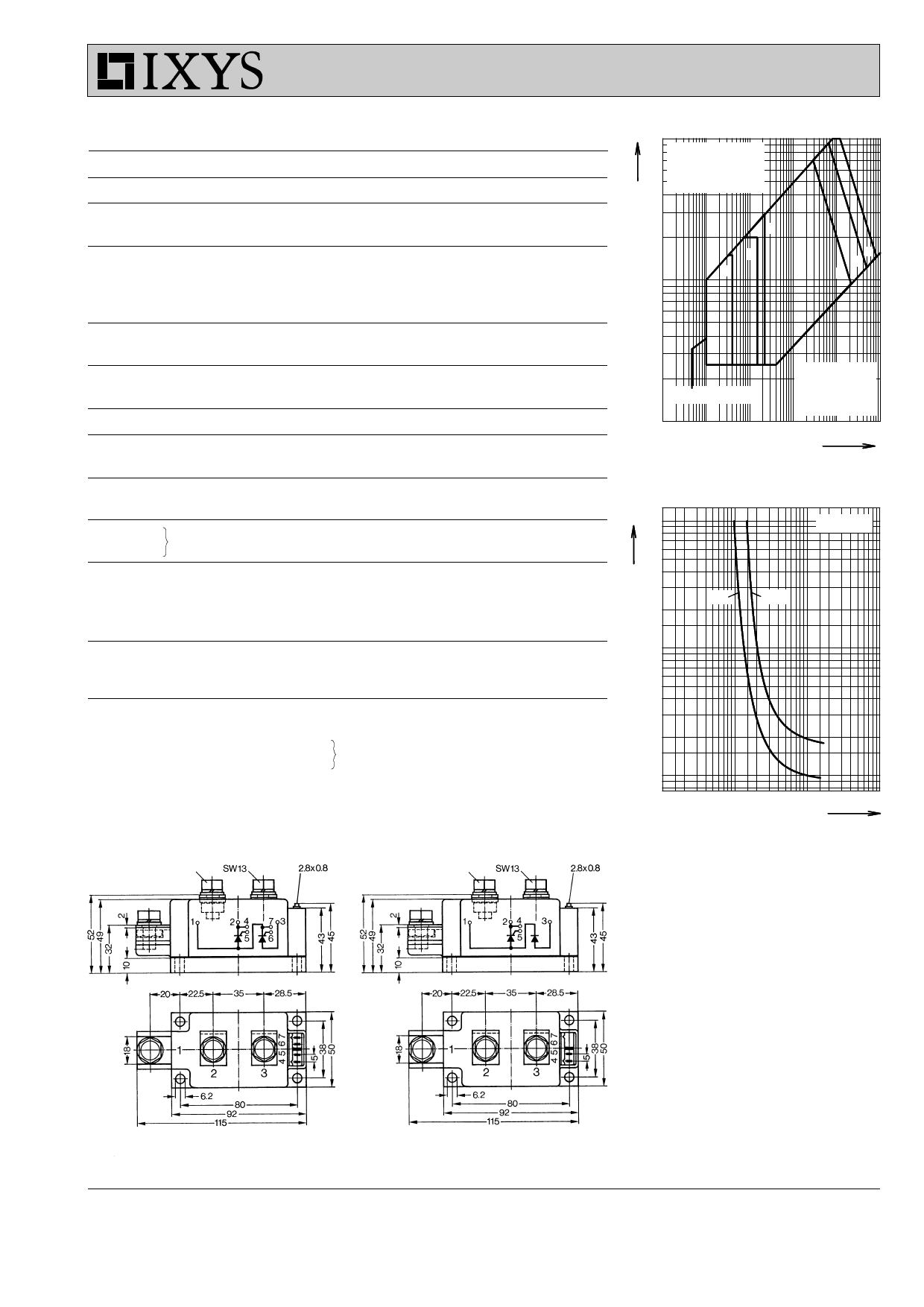
MCD224-20io1
Rectifier
Ratings
Symbol
VRSM/DSM
VRRM/DRM
I R/D
VT
I TAV
I T(RMS)
VT0
rT
R thJC
RthCH
Ptot
I TSM
I²t
CJ
PGM
PGAV
(di/dt)cr
(dv/dt)cr
VGT
IGT
VGD
IGD
IL
IH
t gd
tq
Definition
Conditions
max. non-repetitive reverse/forward blocking voltage
max. repetitive reverse/forward blocking voltage
reverse current, drain current
forward voltage drop
average forward current
RMS forward current
VR/D = 2000 V
VR/D = 2000 V
IT = 250 A
I T = 500 A
IT = 250 A
I T = 500 A
TC = 85°C
180° sine
TVJ = 25°C
TVJ = 25°C
TVJ = 25°C
TVJ = 140°C
TVJ = 25°C
TVJ = 125 °C
TVJ = 140°C
min.
typ. max. Unit
2100 V
2000 V
1 mA
40 mA
1.08 V
1.31 V
1.03 V
1.33 V
250 A
390 A
threshold voltage
slope resistance
for power loss calculation only
TVJ = 140°C
0.72 V
1.2 mΩ
thermal resistance junction to case
0.139 K/W
thermal resistance case to heatsink
0.040
K/W
total power dissipation
max. forward surge current
value for fusing
junction capacitance
max. gate power dissipation
average gate power dissipation
t = 10 ms; (50 Hz), sine
t = 8,3 ms; (60 Hz), sine
t = 10 ms; (50 Hz), sine
t = 8,3 ms; (60 Hz), sine
t = 10 ms; (50 Hz), sine
t = 8,3 ms; (60 Hz), sine
t = 10 ms; (50 Hz), sine
t = 8,3 ms; (60 Hz), sine
VR = 700 V
tP = 30 µs
tP = 500 µs
f = 1 MHz
TC = 25°C
TVJ = 45°C
VR = 0 V
TVJ = 140°C
VR = 0 V
TVJ = 45°C
VR = 0 V
TVJ = 140°C
VR = 0 V
TVJ = 25°C
TC = 140°C
820 W
8.00 kA
8.64 kA
6.80 kA
7.35 kA
320.0 kA²s
310.5 kA²s
231.2 kA²s
224.4 kA²s
235
pF
120 W
60 W
20 W
critical rate of rise of current
critical rate of rise of voltage
gate trigger voltage
gate trigger current
gate non-trigger voltage
gate non-trigger current
TVJ = 125 °C; f = 50 Hz
repetitive, IT = 750 A
tP = 200 µs; diG /dt = 1 A/µs;
IG = 1 A; V = ⅔ VDRM
non-repet., IT = 250 A
V = ⅔ VDRM
TVJ = 125°C
R GK = ∞; method 1 (linear voltage rise)
VD = 6 V
TVJ = 25°C
TVJ = -40°C
VD = 6 V
TVJ = 25°C
TVJ = -40°C
VD = ⅔ VDRM
TVJ = 140°C
100 A/µs
500 A/µs
1000 V/µs
2V
3V
150 mA
220 mA
0.25 V
10 mA
latching current
holding current
gate controlled delay time
turn-off time
t p = 30 µs
TVJ = 25 °C
IG = 0.45 A; diG/dt = 0.45 A/µs
VD = 6 V RGK = ∞
TVJ = 25 °C
VD = ½ VDRM
TVJ = 25 °C
IG = 0.5 A; diG/dt = 0.5 A/µs
VR = 100 V; IT = 250 A; V = ⅔ VDRM TVJ =125 °C
di/dt = 10 A/µs dv/dt = 50 V/µs tp = 200 µs
200 mA
150 mA
2 µs
350
µs
IXYS reserves the right to change limits, conditions and dimensions.
© 2017 IXYS all rights reserved
Data according to IEC 60747and per semiconductor unless otherwise specified
20170116h
Share Link: 