AS4LC1M16883C-8 Ver la hoja de datos (PDF) - Austin Semiconductor
Número de pieza
componentes Descripción
Fabricante
AS4LC1M16883C-8 Datasheet PDF : 22 Pages
| |||
AUSTIN SEMICONDUCTOR, INC.
AS4LC1M16 883C
1 MEG x 16 DRAM
PRELIMINARY
GENERAL DESCRIPTION (continued)
The ?C?A/S/L and ?C?A/S?H inputs internally generate a ?C?A/S
signal functioning in a similar manner to the single
?C?A/S input of other DRAMs. The key difference is each
?C?A/S input ( ?C?A/S/L and ?C?A/S?H ) controls its corresponding
8 DQ inputs during WRITE accesses. ?C?A/S/L controls DQ1
through DQ8 and ?C?A/S?H controls DQ9 through DQ16. The
two ?C?A/S controls give the MT4LC1M16E5(S) both BYTE
READ and BYTE WRITE cycle capabilities.
A logic HIGH on ?W/E dictates READ mode while a logic
LOW on ?W/E dictates WRITE mode. During a WRITE cycle,
data-in (D) is latched by the falling edge of WE or ?C?A/S
(?C?AS/ /L or ?C?A/S/H), whichever occurs last. An EARLY WRITE
occurs when WE is taken LOW prior to either ?C?A/S falling.
A LATE WRITE or READ-MODIFY-WRITE occurs when
WE falls after ?C?A/S (?C?A/S/L or ?C?A/S/H) was taken LOW.
During EARLY WRITE cycles, the data-outputs (Q) will
remain High-Z regardless of the state of ?O/E. During LATE
WRITE or READ-MODIFY-WRITE cycles, ?O/E must be
taken HIGH to disable the data-outputs prior to applying
input data. If a LATE WRITE or READ-MODIFY-WRITE is
attempted while keeping ?O/E LOW, no write will occur, and
the data-outputs will drive read data from the accessed
location.
The 16 data inputs and 16 data outputs are routed through
16 pins using common I/O. Pin direction is controlled by
?O/E and ?W/E.
PAGE ACCESS
PAGE operations allow faster data operations (READ,
WRITE or READ-MODIFY-WRITE) within a row-address-
defined page boundary. The PAGE cycle is always initiated
with a row-address strobed-in by ?R?A/S followed by a col-
umn-address strobed-in by C? ?A/S. ?C?A/S may be toggled-in
by holding ?R?A/S LOW and strobing-in different column-
addresses, thus executing faster memory cycles. Returning
?R?A/S HIGH terminates the PAGE MODE of operation.
EDO PAGE MODE
The AS4LC1M16 provides EDO PAGE MODE which is
an accelerated FAST PAGE MODE cycle. The primary
advantage of EDO is the availability of data-out even after
?C?A/S returns HIGH. EDO provides for ?C?A/S precharge time
(tCP) to occur without the output data going invalid. This
elimination of ?C?A/S output control provides for pipeline
READs.
FAST-PAGE-MODE DRAMs have traditionally turned
the output buffers off (High-Z) with the rising edge of
?C?A/S. EDO-PAGE-MODE DRAMs operate similar to
FAST-PAGE-MODE DRAMs, except data will remain valid
or become valid after ?C?A/S goes HIGH during READs,
provided ?R?A/S and ?O/E are held LOW. If ?O/E is pulsed while
?R?A/S and ?C?A/S are LOW, data will toggle from valid data to
High-Z and back to the same valid data. If ?O/E is toggled or
pulsed after ?C?A/S goes HIGH while ?R?A/S remains LOW, data
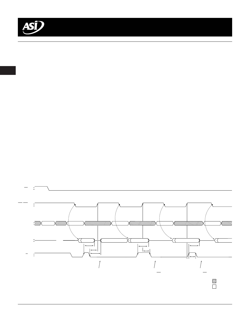
will transition to and remain High-Z (refer to Figure 1).
RAS
V
V
IH
IL
CASL/CASH
V
V
IH
IL
,, ,,, ,,,,,,, ,,,,,,, ,,,,,, ,,,,, ADDR
V
V
IH
IL
ROW
COLUMN (A)
COLUMN (B)
COLUMN (C)
COLUMN (D)
DQ
V
V
IOH
IOL
OPEN
,,VALID DATA (A)
tOD
tOES
VALID DATA (A)
,,, VALID DATA (B)
tOD
tOEHC
,,VALID DATA (C)
tOD
,VALID DATA (D)
OE
V
V
IH
IL
tOE
tOEP
The DQs go back to
Low-Z if tOES is met.
The DQs remain High-Z
until the next CAS cycle
if tOEHC is met.
Figure 1
OUTPUT ENABLE AND DISABLE
The DQs remain High-Z
until the next CAS cycle
, if tOEP is met.
DON’T CARE
,,,,,UNDEFINED
AS4LC1M16
REV. 3/97
DS000020
2-94
Austin Semiconductor, Inc., reserves the right to change products or specifications without notice.
Share Link: 