4N37-X Ver la hoja de datos (PDF) - Vishay Semiconductors
Número de pieza
componentes Descripción
Fabricante
4N37-X Datasheet PDF : 7 Pages
| |||
www.vishay.com
4N35-X, 4N36-X, 4N37-X, 4N38
Vishay Semiconductors
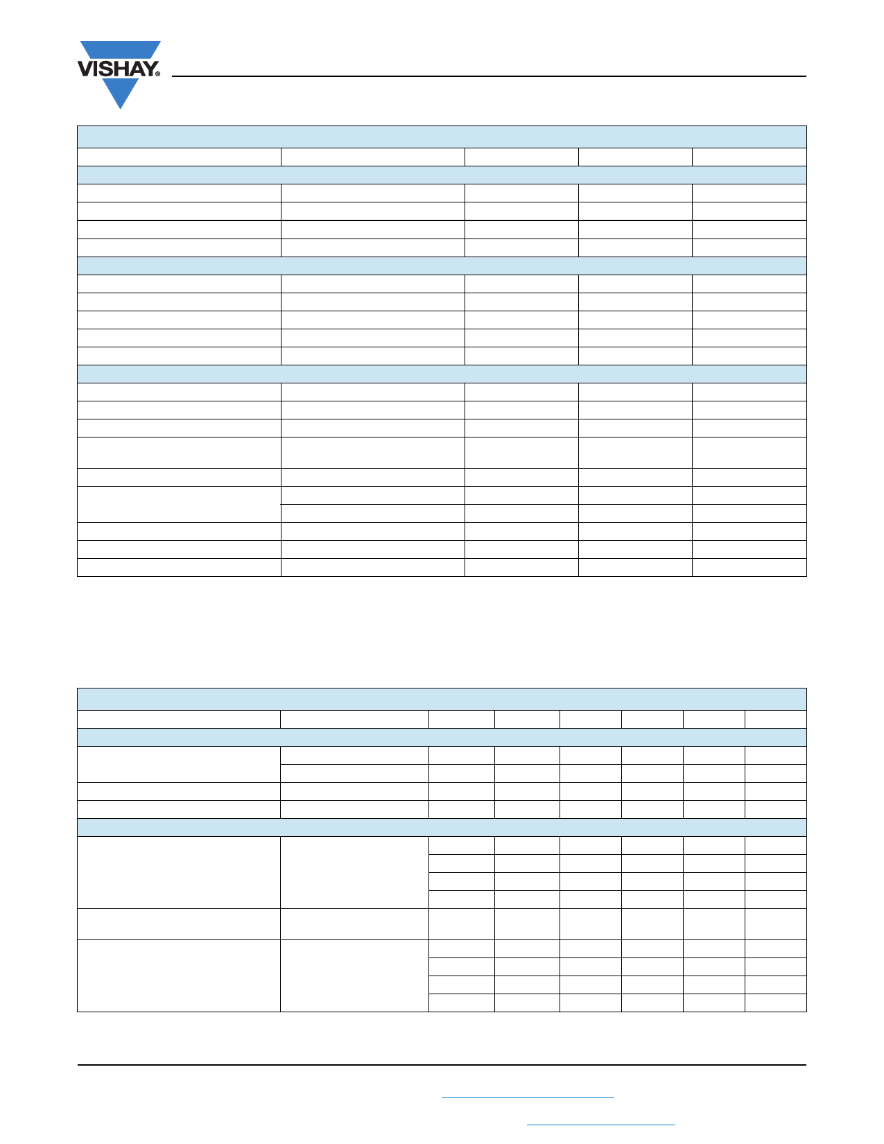
ABSOLUTE MAXIMUM RATINGS (Tamb = 25 °C, unless otherwise specified)
PARAMETER
TEST CONDITION
SYMBOL
VALUE
UNIT
INPUT
Reverse voltage
Forward current
Surge current
Power dissipation
OUTPUT
t ≤ 10 μs
VR
6
V
IF
60
mA
IFSM
2.5
A
Pdiss
70
mW
Collector emitter breakdown voltage
VCEO
70
V
Emitter base breakdown voltage
VEBO
7
V
Collector current
IC
50
mA
Collector peak current
tp/T = 0.5, tp ≤ 10 ms
ICM
100
mA
Output power dissipation
Pdiss
150
mW
COUPLER
Isolation test voltage
Creepage distance
t=1s
VISO
5000
≥7
VRMS
mm
Clearance distance
≥7
mm
Isolation thickness between emitter
and detector
≥ 0.4
mm
Comparative tracking index
DIN IEC 112/VDE 0303, part 1
≥ 175
Isolation resistance
Storage temperature
Operating temperature
Soldering temperature (1)
VIO = 500 V, Tamb = 25 °C
RIO
≥ 1012
Ω
VIO = 500 V, Tamb = 100 °C
RIO
≥ 1011
Ω
Tstg
- 55 to + 150
°C
Tamb
- 55 to + 100
°C
2 mm from case, ≤ 10 s
Tsld
260
°C
Notes
• Stresses in excess of the absolute maximum ratings can cause permanent damage to the device. Functional operation of the device is not
implied at these or any other conditions in excess of those given in the operational sections of this document. Exposure to absolute
maximum ratings for extended periods of the time can adversely affect reliability.
(1) Refer to reflow profile for soldering conditions for surface mounted devices (SMD). Refer to wave profile for soldering condditions for through
hole devices (DIP).
ELECTRICAL CHARACTERISTICS (Tamb = 25 °C, unless otherwise specified)
PARAMETER
TEST CONDITION
PART SYMBOL MIN.
INPUT
Forward voltage (1)
Reverse current (1)
Capacitance
OUTPUT
IF = 10 mA
IF = 10 mA, Tamb = - 55 °C
VR = 6 V
VR = 0 V, f = 1 MHz
VF
VF
0.9
IR
CO
Collector emitter breakdown
voltage (1)
Emitter collector breakdown
voltage (1)
IC = 1 mA
IE = 100 μA
4N35
BVCEO
30
4N36
BVCEO
30
4N37
BVCEO
30
4N38
BVCEO
80
BVECO
7
Collector base breakdown
voltage (1)
4N35
BVCBO
70
IC = 100 μA, IB = 1 μA
4N36
4N37
BVCBO
BVCBO
70
70
4N38
BVCBO
80
TYP.
1.2
1.3
0.1
25
MAX.
1.5
1.7
10
UNIT
V
V
μA
pF
V
V
V
V
V
V
V
V
V
Rev. 1.8, 16-Jan-12
2
Document Number: 83717
For technical questions, contact: optocoupleranswers@vishay.com
THIS DOCUMENT IS SUBJECT TO CHANGE WITHOUT NOTICE. THE PRODUCTS DESCRIBED HEREIN AND THIS DOCUMENT
ARE SUBJECT TO SPECIFIC DISCLAIMERS, SET FORTH AT www.vishay.com/doc?91000
Share Link: 