M48Z128 Ver la hoja de datos (PDF) - STMicroelectronics
Número de pieza
componentes Descripción
Fabricante
M48Z128 Datasheet PDF : 17 Pages
| |||
M48Z128, M48Z128Y
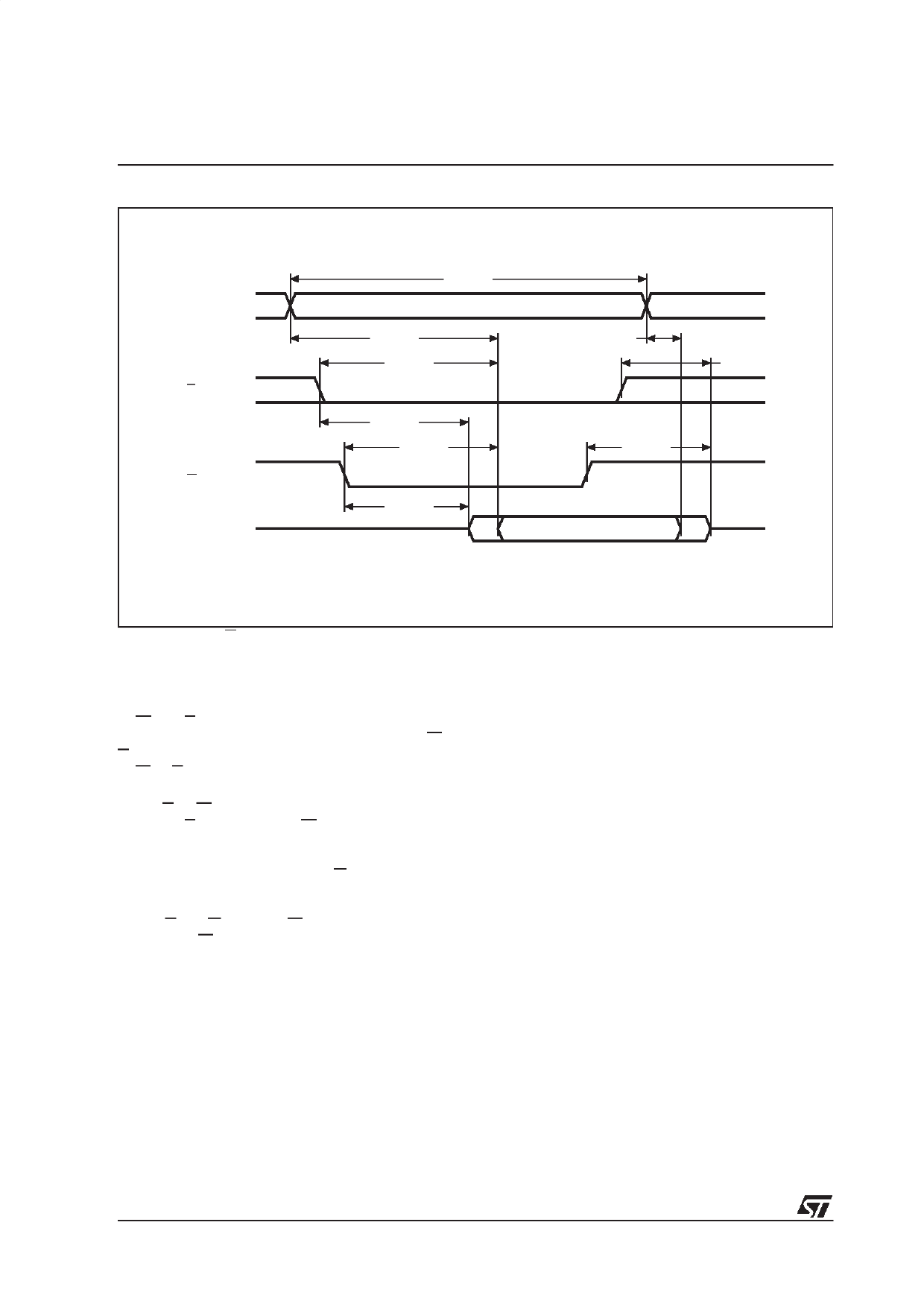
Figure 8. Chip Enable or Output Enable Controlled, Read Mode AC Waveforms
A0-A16
E
G
DQ0-DQ7
tAVQV
tELQV
tAVAV
VALID
tELQX
tGLQV
tGLQX
tAXQX
tEHQZ
tGHQZ
DATA OUT
AI01197
Note: Write Enable (W) = High.
WRITE MODE
The M48Z128/128Y is in the Write Mode whenev-
er W and E are active. The start of a write is refer-
enced from the latter occurring falling edge of W or
E. A write is terminated by the earlier rising edge
of W or E.
The addresses must be held valid throughout the
cycle. E or W must return high for minimum of tE-
HAX from E or tWHAX from W prior to the initiation
of another read or write cycle. Data-in must be val-
id tDVWH prior to the end of write and remain valid
for tWHDX or tEHDX afterward. G should be kept
high during write cycles to avoid bus contention;
although, if the output bus has been activated by a
low on E and G, a low on W will disable the outputs
tWLQZ after W falls.
DATA RETENTION MODE
With
ates
avsalaidcVoCnvCeanptipolnieadl ,BtYhTeEMW4I8DZE1T2M8/s1t2a8tiYc
oper-
RAM.
Should the supply voltage decay, the RAM will au-
tomatically power-fail deselect, write protecting it-
self tWP after VCC falls below VPFD. All outputs
become high impedance, and all inputs are treated
as ”don’t care.”
If power fail detection occurs during a valid ac-
cess, the memory cycle continues to completion. If
the memory cycle fails to terminate within the time
tWP, write protection takes place. When VCC drops
below VSO, the control circuit switches power to
the internal energy source which preserves data.
The internal coin cell will maintain data in the
M48Z128/128Y after the initial application of VCC
for an accumulated period of at least 10 years
when VCC is less than VSO. As system power re-
turns and VCC rises above VSO, the battery is dis-
connected, and the power supply is switched to
external VCC. Write protection continues for tER af-
ter VCC reaches VPFD to allow for processor stabi-
lization. After tER, normal RAM operation can
resume.
For more information on Battery Storage Life refer
to the Application Note AN1012.
8/17
Share Link: 