2SK1519-E Ver la hoja de datos (PDF) - Renesas Electronics
Número de pieza
componentes Descripción
Fabricante
2SK1519-E Datasheet PDF : 7 Pages
| |||
2SK1519, 2SK1520
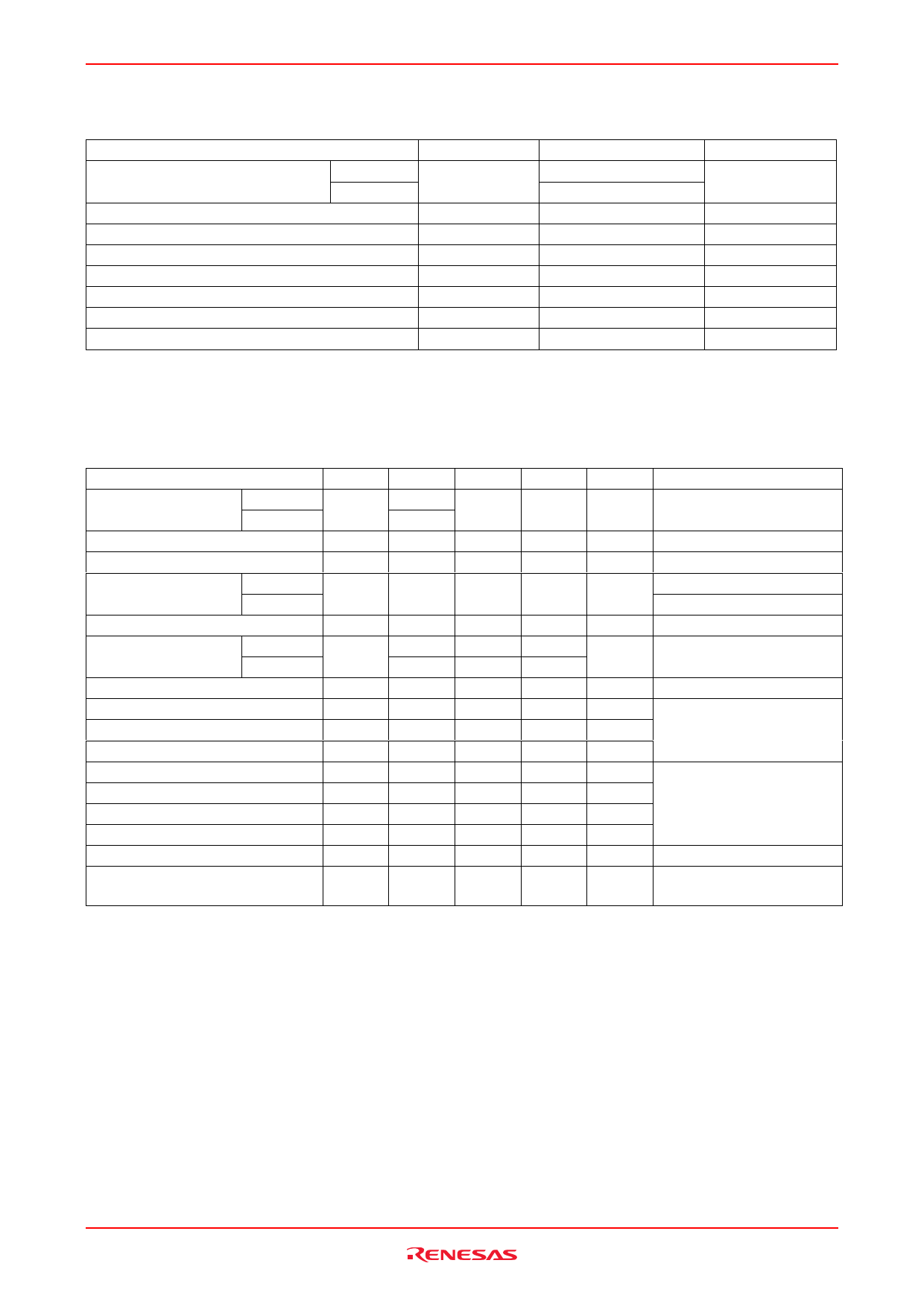
Absolute Maximum Ratings
Item
Drain to source voltage
2SK1519
2SK1520
Gate to source voltage
Drain current
Drain peak current
Body to drain diode reverse drain current
Channel dissipation
Channel temperature
Storage temperature
Notes: 1. PW ≤ 10 µs, duty cycle ≤ 1%
2. Value at TC = 25°C
Electrical Characteristics
Symbol
VDSS
VGSS
ID
ID(pulse)*1
IDR
Pch*2
Tch
Tstg
Item
Symbol Min
Drain to source
breakdown voltage
2SK1519
V(BR)DSS
450
2SK1520
500
Gate to source breakdown voltage V(BR)GSS ±30
Gate to source leak current
IGSS
—
Zero gate voltage drain 2SK1519
IDSS
—
current
2SK1520
Gate to source cutoff voltage
VGS(off)
2.0
Static drain to source on 2SK1519
RDS(on)
—
state resistance
2SK1520
—
Forward transfer admittance
|yfs|
15
Input capacitance
Ciss
—
Output capacitance
Coss
—
Reverse transfer capacitance
Crss
—
Turn-on delay time
td(on)
—
Rise time
tr
—
Turn-off delay time
td(off)
—
Fall time
tf
—
Body to drain diode forward voltage
VDF
—
Body to drain diode reverse recovery trr
—
time
Note: 3. Pulse test
Typ
—
—
—
—
—
0.11
0.12
25
5800
1550
170
65
170
415
200
1.1
120
Ratings
450
500
±30
30
120
30
200
150
–55 to +150
(Ta = 25°C)
Unit
V
V
A
A
A
W
°C
°C
Max
—
—
±10
250
3.0
0.15
0.16
—
—
—
—
—
—
—
—
—
—
(Ta = 25°C)
Unit
Test conditions
V ID = 10 mA, VGS = 0
V IG = ±100 µA, VDS = 0
µA VGS = ±25 V, VDS = 0
µA VDS = 360 V, VGS = 0
VDS = 400 V, VGS = 0
V ID = 1 mA, VDS = 10 V
Ω
ID = 15 A, VGS = 10 V *3
S
ID = 15 A, VDS = 10 V *3
pF VDS = 10 V, VGS = 0,
pF f = 1 MHz
pF
ns ID = 15 A, VGS = 10 V,
ns RL = 2 Ω
ns
ns
V IF = 30 A, VGS = 0
ns IF = 30 A, VGS = 0,
diF/dt = 100 A/µs
Rev.3.00 Apr 27, 2006 page 2 of 6
Share Link: 