2SJ567(2002) Ver la hoja de datos (PDF) - Toshiba
Número de pieza
componentes Descripción
Fabricante
2SJ567 Datasheet PDF : 6 Pages
| |||
2SJ567
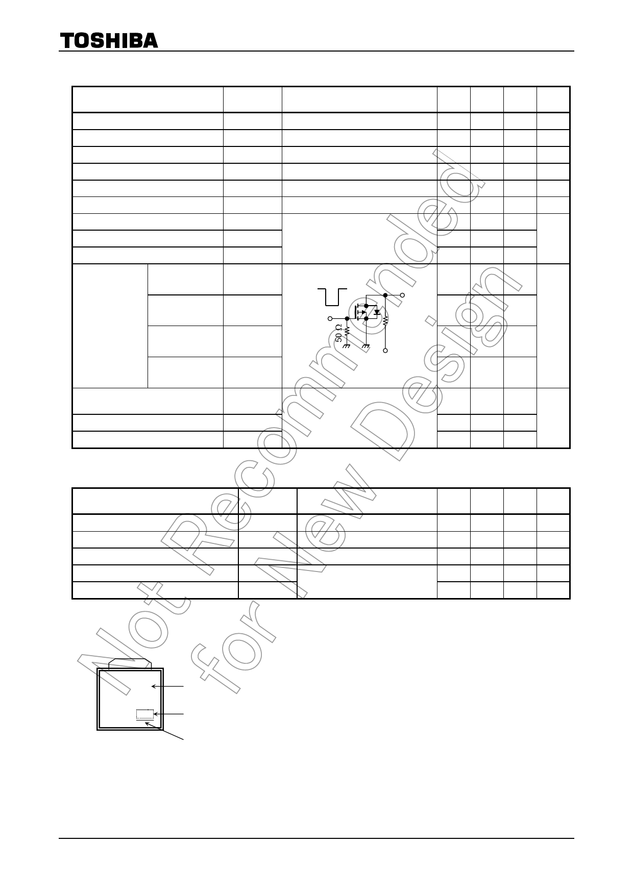
Electrical Characteristics (Ta = 25°C)
Characteristics
Gate leakage current
Drain cut-off current
Drain-source breakdown voltage
Gate threshold voltage
Drain-source ON resistance
Forward transfer admittance
Input capacitance
Reverse transfer capacitance
Output capacitance
Rise time
Switching time
Turn-on time
Fall time
Turn-off time
Total gate charge
(Gate source plus gate-drain)
Gate-source charge
Gate-drain (“Miller”) charge
Symbol
Test Condition
Min Typ. Max Unit
IGSS
IDSS
V (BR) DSS
Vth
RDS (ON)
ïYfsï
Ciss
Crss
Coss
VGS = ±16 V, VDS = 0 V
VDS = -200 V, VGS = 0 V
ID = -10 mA, VGS = 0 V
VDS = -10 V, ID = -1 mA
VGS = -10 V, ID = -1.5 A
VDS = -10 V, ID = -1.5 A
VDS = -10 V, VGS = 0 V, f = 1 MHz
¾
¾
±10
mA
¾
¾ -100 mA
-200 ¾
¾
V
-1.5
¾ -3.5
V
¾
1.6 2.0
W
1.0
2.0
¾
S
¾
410
¾
¾
40
¾
pF
¾ 145 ¾
tr
0V
VGS
ton
-10 V
ID = -1.5 A VOUT
¾
20
¾
¾
45
¾
RL = 66.7 W
ns
tf
¾
15
¾
toff
Duty <= 1%, tw = 10 ms VDD ~- -100 V
¾
85
¾
Qg
VDD ~- -160 V, VGS = -10 V,
Qgs
ID = -2.5 A
Qgd
¾
10
¾
¾
6
¾
nC
¾
4
¾
Source-Drain Ratings and Characteristics (Ta = 25°C)
Characteristics
Continuous drain reverse current
(Note 1)
Pulse drain reverse current
(Note 1)
Forward voltage (diode)
Reverse recovery time
Reverse recovery charge
Symbol
IDR
IDRP
VDSF
trr
Qrr
Test Condition
¾
¾
IDR = -2.5 A, VGS = 0 V
IDR = -2.5 A, VGS = 0 V,
dIDR/dt = 100 A/ms
Min Typ. Max Unit
¾
¾
-2.5
A
¾
¾
-10
A
¾
¾
2.0
V
¾
135
¾
ns
¾ 0.81 ¾
mC
Marking
J567
※
Type
※ Lot Number
Month (starting from alphabet A)
Year (last number of the christian era)
2
2002-08-12
Share Link: 