SA8026DH Ver la hoja de datos (PDF) - Philips Electronics
Número de pieza
componentes Descripción
Fabricante
SA8026DH Datasheet PDF : 18 Pages
| |||
Philips Semiconductors
2.5GHz low voltage fractional-N dual frequency
synthesizer
Product specification
SA8026
CHARACTERISTICS (continued)
SYMBOL
PARAMETER
CONDITIONS
Phase noise (condition RSET = 7.5 kΩ, CP = 00)
Synthesizer’s contribution to close-in phase noise
of 900 MHz RF signal at 1 kHz offset.
Synthesizer’s contribution to close-in phase noise
of 1800 MHz RF signal at 1 kHz offset.
L(f)
Synthesizer’s contribution to close-in phase noise
of 800 MHz RF signal at 1 kHz offset.
Synthesizer’s contribution to close-in phase noise
of 2100 MHz RF signal at 1 kHz offset.
GSM
fREF = 13MHz, TCXO,
fCOMP = 1MHz
indicative, not tested
TDMA
fREF = 19.44MHz, TCXO,
fCOMP = 240kHz
indicative, not tested
Interface logic input signal levels; pins 2, 17, 18, 19, 20
VIH
VIL
ILEAK
HIGH level input voltage
LOW level input voltage
Input leakage current
Lock detect output signal (in push/pull mode); pin 1
VOL
LOW level output voltage
VOH
HIGH level output voltage
NOTES:
1.
ISET
=
VSET
RSET
bias
current
for
charge
pumps.
logic 1 or logic 0
Isink = 2mA
Isource = –2mA
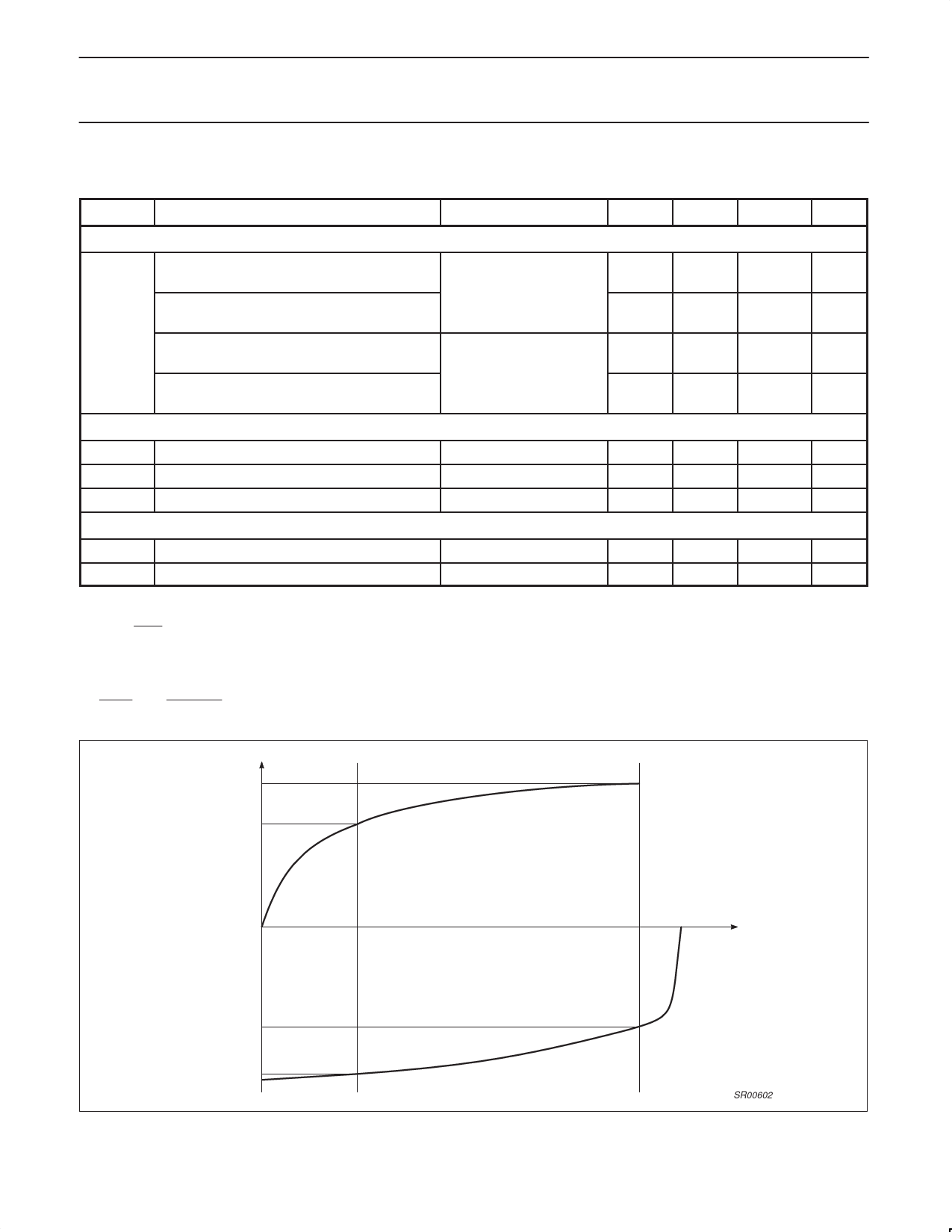
2. The relative output current variation is defined as:
DIOUT
IOUT
+
2.
(I2–I1)
I(I2 ) I1)I
;
with V1 + 0.7V,
V2 + VDDCP –0.8V (See Figure 3.)
MIN.
TYP.
–
–90
–
–83
–
–85
–
–77
0.7*VDD
–
–0.3
–
–0.5
–
–
–
VDD–0.4
–
MAX.
UNIT
–
dBc/Hz
–
dBc/Hz
–
dBc/Hz
–
dBc/Hz
VDD+0.3
V
0.3*VDD
V
+0.5
µA
0.4
V
–
V
IZOUT
CURRENT
I2
I1
1999 Nov 04
V1
V2
VPH
I2
I1
Figure 3. Relative Output Current Variation
6
SR00602
Share Link: 