AD8346 Ver la hoja de datos (PDF) - Analog Devices
Número de pieza
componentes Descripción
Fabricante
AD8346 Datasheet PDF : 20 Pages
| |||
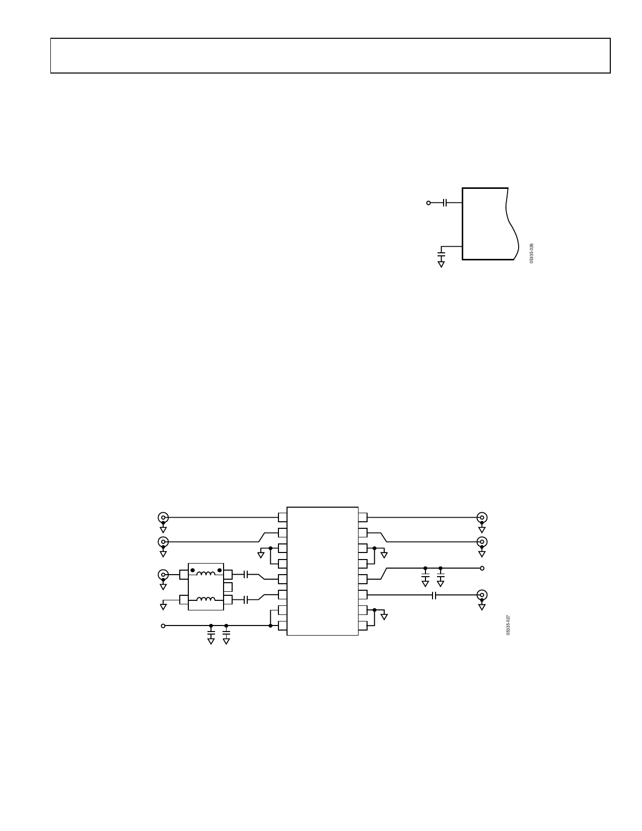
BASIC CONNECTIONS
The basic connections for operating the AD8346 are shown in
Figure 27. A single power supply of between 2.7 V and 5.5 V is
applied to pins VPS1 and VPS2. A pair of ESD protection
diodes are connected internally between VPS1 and VPS2 so
these must be tied to the same potential. Both pins should be
individually decoupled using 100 pF and 0.01 μF capacitors,
located as close as possible to the device. For normal operation,
the enable pin, ENBL, must be pulled high. The turn-on
threshold for ENBL is 2 V. To put the device in its power-down
mode, ENBL must be pulled below 0.5 V. Pins COM1 to COM4
should all be tied to a low impedance ground plane.
The I and Q ports should be driven differentially. This is con-
venient as most modern high speed DACs have differential
outputs. For optimal performance, the drive signal should be a
2 V p-p (differential) signal with a bias level of 1.2 V, that is,
each input swings from 0.7 V to 1.7 V. The I and Q inputs have
input impedances of 12 kΩ. By dc coupling the DAC to the
AD8346 and applying small offset voltages, the LO feedthrough
can be reduced to well below its nominal value of −42 dBm
(see Figure 12).
LO DRIVE
The return loss of the LO port is shown in Figure 18. No add-
itional matching circuitry is required to drive this port from a
50 Ω source. For maximum LO suppression at the output, a
differential LO drive is recommended. In Figure 27, this is
achieved using a balun (M/A-COM Part Number ETC1-1-13).
The output of the balun is ac-coupled to the LO inputs which
AD8346
have a bias level about 800 mV below supply. An LO drive
level of between −6 dBm and −12 dBm is required. For optimal
performance, a drive level of −10 dBm is recommended,
although a level of −6 dBm results in more stable temperature
performance (see Figure 8). Higher levels degrade linearity
while lower levels tend to increase the noise floor.
100pF
LO
LOIP
AD8346
100pF
LOIN
Figure 26. Single-Ended LO Drive
The LO terminal can be driven single-ended, as shown in
Figure 26 at the expense of slightly higher LO feedthrough.
LOIN is ac coupled to ground using a capacitor and LOIP is
driven through a coupling capacitor from a (single-ended)
50 Ω source (this scheme could also be reversed with LOIP
being ac-coupled to ground).
RF OUTPUT
The RF output is designed to drive a 50 Ω load, but must be ac-
coupled, as shown in Figure 27. If the I and Q inputs are driven
in quadrature by 2 V p-p signals, the resulting output power is
about −10 dBm (see Figure 7 for variations in output power
over frequency).
IP
IN
C6
100pF
LO
5
1
T1
ETC1-1-13 2
C7
100pF
4
3
+VS
C4
C3
0.01μF
100pF
1 IBBP
QBBP 16
2 IBBN
QBBN 15
AD8346
3 COM1
COM4 14
4 COM1
COM4 13
5 LOIN
VPS2 12
6 LOIP
VOUT 11
7 VPS1
COM3 10
8 ENBL
COM2 9
QP
QN
C1
100pF
C2
0.01μF
C5
100pF
+VS
VOUT
Figure 27. Basic Connections
Rev. A | Page 11 of 20
Share Link: 