27LV64 Ver la hoja de datos (PDF) - Microchip Technology
Número de pieza
componentes Descripción
Fabricante
27LV64 Datasheet PDF : 10 Pages
| |||
27LV64
1.3 Standby Mode
The standby mode is defined when the CE pin is high
(VIH) and a program mode is not defined.
When these conditions are met, the supply current will
drop from 20 mA to 100 µA.
1.4 Output Enable
This feature eliminates bus contention in microproces-
sor-based systems in which multiple devices may drive
the bus. The outputs go into a high impedance state
when the following condition is true:
• The OE and PGM pins are both high.
1.5 Erase Mode (U.V. Windowed
Versions)
Windowed products offer the capability to erase the
memory array. The memory matrix is erased to the all
1’s state when exposed to ultraviolet light. To ensure
complete erasure, a dose of 15 watt-second/cm2 is
required. This means that the device window must be
placed within one inch and directly underneath an ultra-
violet lamp with a wavelength of 2537 Angstroms,
intensity of 12,000µW/cm2 for approximately 20 min-
utes.
1.6 Programming Mode
The Express Algorithm has been developed to improve
the programming throughput times in a production
environment. Up to ten 100-microsecond pulses are
applied until the byte is verified. No overprogramming
is required. A flowchart of the express algorithm is
shown in Figure 1-3.
Programming takes place when:
a) VCC is brought to the proper voltage,
b) VPP is brought to the proper VH level,
c) the CE pin is low,
d) the OE pin is high, and
e) the PGM pin is low.
Since the erased state is “1” in the array, programming
of “0” is required. The address to be programmed is set
via pins A0-A12 and the data to be programmed is pre-
sented to pins O0-O7. When data and address are sta-
ble, OE is high, CE is low and a low-going pulse on the
PGM line programs that location.
1.7 Verify
After the array has been programmed it must be veri-
fied to ensure all the bits have been correctly pro-
grammed. This mode is entered when all the following
conditions are met:
a) VCC is at the proper level,
b) VPP is at the proper VH level,
c) the CE line is low,
d) the PGM line is high, and
e) the OE line is low.
1.8 Inhibit
When programming multiple devices in parallel with dif-
ferent data, only CE or PGM need be under separate
control to each device. By pulsing the CE or PGM line
low on a particular device in conjunction with the PGM
or CE line low, that device will be programmed; all other
devices with CE or PGM held high will not be pro-
grammed with the data, although address and data will
be available on their input pins (i.e., when a high level
is present on CE or PGM); and the device is inhibited
from programming.
1.9 Identity Mode
In this mode specific data is output which identifies the
manufacturer as Microchip Technology Inc. and device
type. This mode is entered when Pin A9 is taken to VH
(11.5V to 12.5V). The CE and OE lines must be at VIL.
A0 is used to access any of the two non-erasable bytes
whose data appears on O0 through O7.
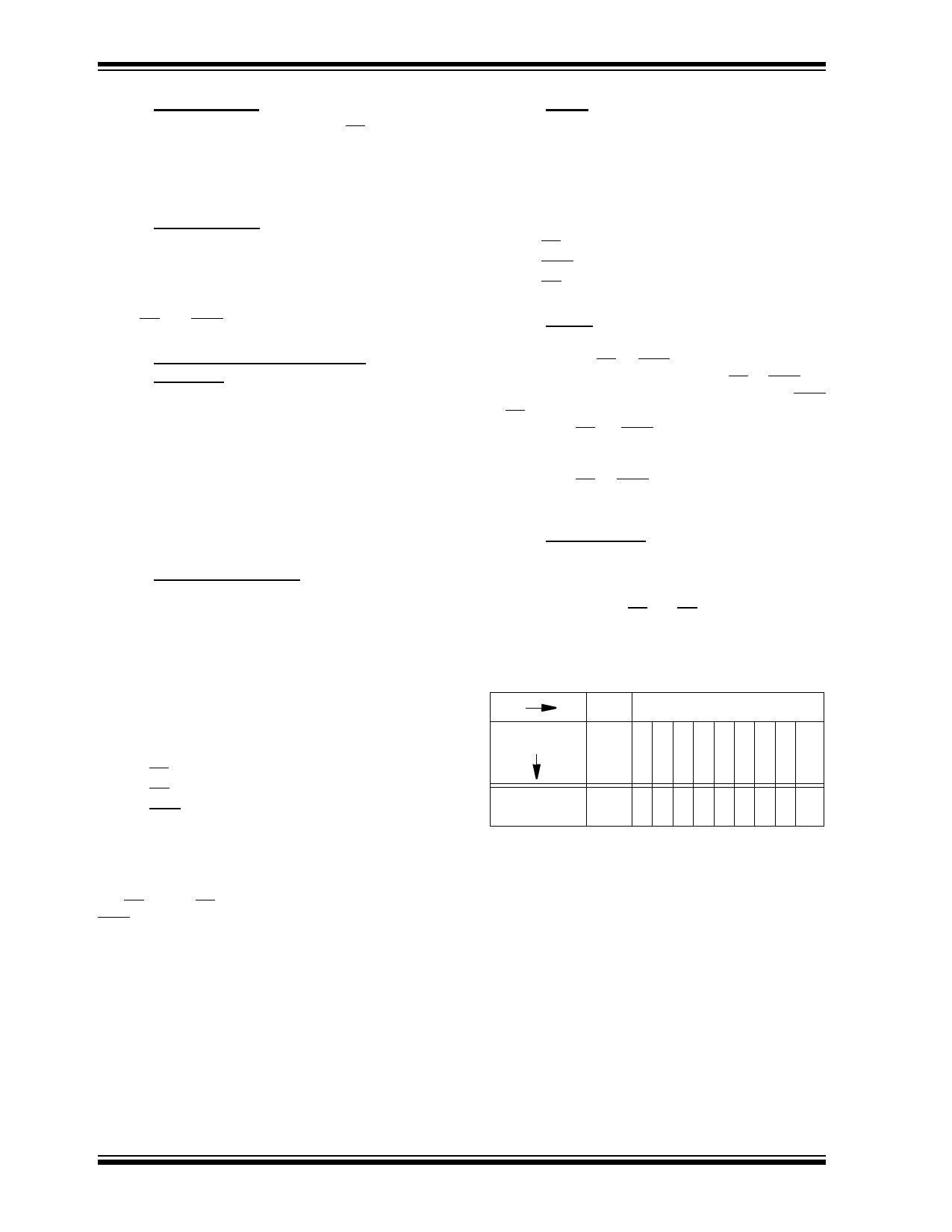
Pin
Input
Output
Identity
A0
0 OOOOOOO
76543210
H
e
x
Manufacturer VIL 0 0 1 0 1 0 0 1 29
Device Type* VIH 0 0 0 0 0 0 1 0 02
* Code subject to change
DS11024F-page 6
2004 Microchip Technology Inc.
Share Link: 