27C256-30I Ver la hoja de datos (PDF) - Microchip Technology
Número de pieza
componentes Descripción
Fabricante
27C256-30I Datasheet PDF : 10 Pages
| |||
27LV256
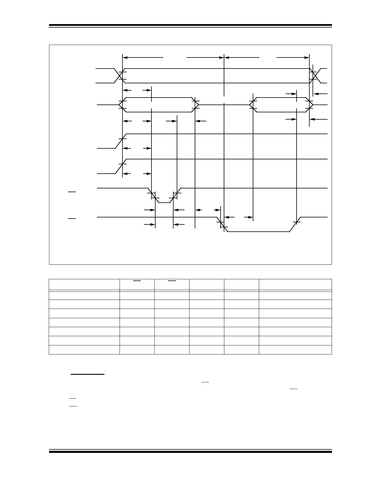
FIGURE 1-2: PROGRAMMING WAVEFORMS
V IH
Address
V IL
V IH
Data
V IL
13.0V(2)
V PP
5.0V
6.5V(2)
V CC
5.0V
V IH
CE
V IL
V IH
OE
V IL
Program
Address Stable
t AS
Data Stable
t DS
t DH
t VPS
t VCS
High Z
Verify
t AH
Data Out Valid
t DF
(1)
t PW
t OPW
t OES
t OE
(1)
Notes:
(1) tDF and t OE are characteristics of the device but must be accommodated by the programmer
(2) VCC = 6.5V ±0.25V, V PP = V H = 13.0V ±0.25V for express algorithm
TABLE 1-6: MODES
Operation Mode
Read
Program
Program Verify
Program Inhibit
Standby
Output Disable
Identity
X = Don’t Care
CE
OE
VIL
VIL
VIL
VIH
VIH
VIL
VIH
VIH
VIH
X
VIL
VIH
VIL
VIL
1.2 Read Mode
(See Timing Diagrams and AC Characteristics)
Read Mode is accessed when:
a) the CE pin is low to power up (enable) the chip
b) the OE pin is low to gate the data to the output
pins
VPP
A9
VCC
X
VH
X
VH
X
VH
X
VCC
X
VCC
X
VCC
VH
O0 - O7
DOUT
DIN
DOUT
High Z
High Z
High Z
Identity Code
For Read operations, if the addresses are stable, the
address access time (tACC) is equal to the delay from
CE to output (tCE). Data is transferred to the output
after a delay from the falling edge of OE (tOE).
2004 Microchip Technology Inc.
DS11020H-page 5
Share Link: 