28F002BC Ver la hoja de datos (PDF) - Intel
Número de pieza
componentes Descripción
Fabricante
28F002BC Datasheet PDF : 37 Pages
| |||
28F002BC 2-MBIT BOOT BLOCK FLASH MEMORY
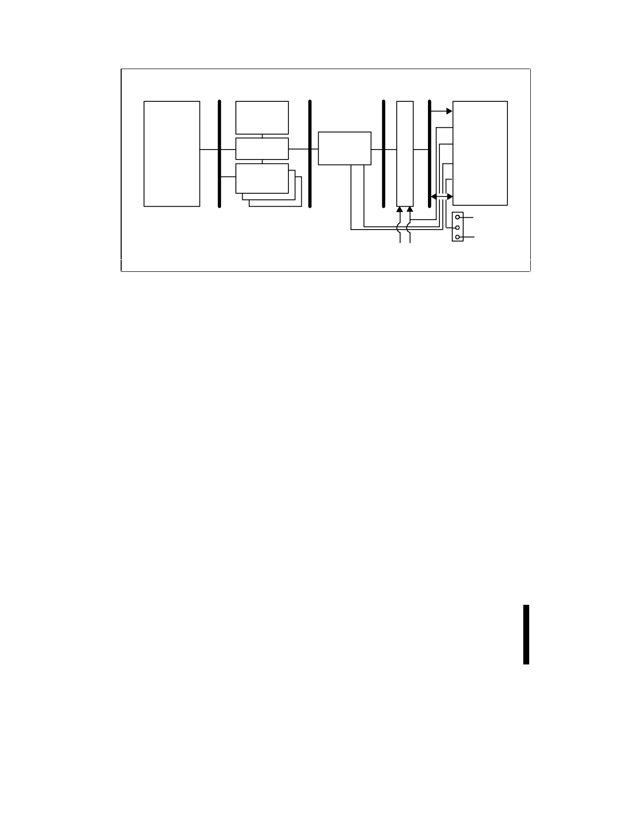
E
Pentium®
Processor
100/90 MHz
Host
Bus
Main
Memory
82430FX
PCIset
(82437FX)
Cache
PCI
Bus
ISA
Bus
X-Bus
A[16:0]
7B
82430FX
4U
PCIset
SF
(82371FB)
2F
4E
XX
MM
5R
EE
MM
WR
##
CE#
OE# Intel
28F002BC
WE#
RP#
DQ[7:0]
PWROK
XDIR XOE#
Vpp
J1
0578_01
Figure 1. 28F002BC-T Interface to a Pentium® Microprocessor System
IPP, the maximum program current, is 20 mA. The
VPP voltage for erase and program is 11.4V to
12.6V (VPP = 12V ± 5%) under all operating
conditions. Typical ICC active current is 20 mA.
The 28F002BC flash memory is also designed with
a standby mode to minimize system current drain
and allow for low-power designs. When the CE#
and RP# pins are at VCC, the CMOS standby mode
is enabled and ICC drops to about 50 µA.
A deep power-down mode is enabled when the RP#
pin is at ground. In addition to minimizing power
consumption, the deep power-down mode also
provides write protection during power-up
conditions. ICC current during deep power-down
mode is 0.20 µA typical. An initial maximum access
time or reset time of 300 ns is required from RP#
switching high until outputs are valid. Equivalently,
the device has a maximum wake-up time of 215 ns
until writes to the CUI are recognized.
When RP# is at ground, the WSM is reset, the
status register is cleared, and the entire device is
write-protected. This feature prevents data
corruption and protects the code stored in the
device during system reset. The system Reset pin
can be tied to RP# to reset the memory to read
mode at power-up. With on-chip program/erase
automation and RP# functionality for data
protection, the device is protected against
unwanted program and/or erase cycles, even
during system reset.
1.3 Applications
2-Mbit Boot Block flash memory combines high
density, high performance, and cost-effective flash
memory with blocking and hardware protection
capabilities. Its flexibility and versatility reduces
cost throughout the product life cycle. Flash
memory is ideal for Just-In-Time production flow,
reducing system inventory and costs, and
eliminating component handling during the
production phase. During a product’s life cycle,
flash memory reduces costs by allowing user-
performed code updates and feature enhancements
via floppy disk or remote link.
The 28F002BC is a full-function blocked flash
product suitable for a wide range of applications,
including extended PC BIOS, digital cellular phone
program and data storage, telecommunication
boot/firmware, and various embedded applications
where both program and data storage are required.
6
PRELIMINARY
Share Link: 