24AA01-/P Ver la hoja de datos (PDF) - Microchip Technology
Número de pieza
componentes Descripción
Fabricante
24AA01-/P Datasheet PDF : 24 Pages
| |||
24AA01/24LC01B
8.0 PIN DESCRIPTIONS
The descriptions of the pins are listed in Table 8-1.
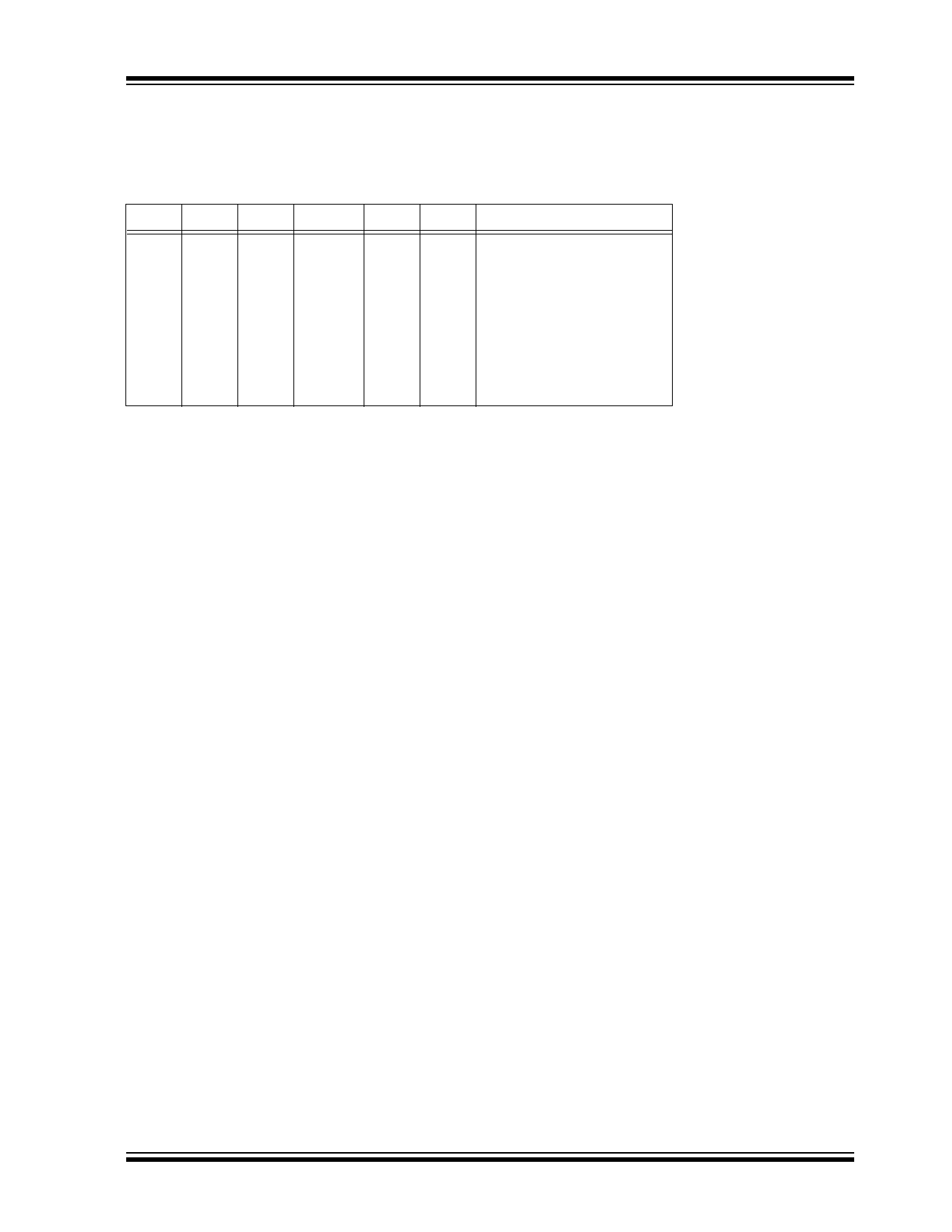
TABLE 8-1: PIN FUNCTION TABLE
Name
A0
A1
A2
VSS
SDA
SCL
WP
VCC
PDIP
1
2
3
4
5
6
7
8
SOIC
1
2
3
4
5
6
7
8
TSSOP
1
2
3
4
5
6
7
8
MSOP SOT23
Description
1
— Not Connected
2
— Not Connected
3
— Not Connected
4
2 Ground
5
3 Serial Address/Data I/O
6
1 Serial Clock
7
5 Write Protect Input
8
4 +1.8V to 5.5V Power Supply
8.1 A0, A1, A2
These pins are not used by the 24XX01. They may be
left floating or tied to either VSS or VCC.
8.2 Serial Address/Data Input/Output
(SDA)
This is a bi-directional pin used to transfer addresses
and data into and data out of the device. It is an open
drain terminal. Therefore, the SDA bus requires a pull-
up resistor to VCC (typical 10 kΩ for 100 kHz, 2 kΩ for
400 kHz).
For normal data transfer SDA is allowed to change only
during SCL LOW. Changes during SCL HIGH are
reserved for indicating the START and STOP condi-
tions.
8.3 Serial Clock (SCL)
This input is used to synchronize the data transfer from
and to the device.
8.4 Write-Protect (WP)
This pin must be connected to either VSS or VCC.
If tied to VSS normal memory operation is enabled
(read/write the entire memory 00-7F).
If tied to VCC, WRITE operations are inhibited. The
entire memory will be write-protected. Read operations
are not affected.
This feature allows the user to use the 24XX01 as a
serial ROM when WP is enabled (tied to VCC).
2002 Microchip Technology Inc.
DS21711A-page 11
Share Link: 