INA-30311-BLK Ver la hoja de datos (PDF) - HP => Agilent Technologies
Número de pieza
componentes Descripción
Fabricante
INA-30311-BLK Datasheet PDF : 6 Pages
| |||
INA-30311 Applications
Information
Introduction
The INA-30311 is a silicon RF
integrated circuit that provides an
easy-to-use solution for low noise
or multi-purpose gain block
applications up to 1000 MHz. This
two-stage amplifier design uses
resistive feedback to provide flat
gain over a wide frequency range.
This device is assembled in a
miniature, surface mount package
and is intended for use in low
cost wireless communication
products.
A unique feature of the INA-30311
is that it is designed with a 50 Ω
input impedance and an output
impedance that approaches 200 Ω
at lower frequencies. This imped-
ance converting feature is very
useful for applications such as
receiver IF circuits in which the
INA-30311 is followed by high
input impedance devices like
signal processing circuits, filters,
or mixed signal ICs.
In addition to simplifying the
match to higher impedance
devices, a key benefit of the
higher output impedance feature
is an improvement in power
efficiency.
Phase Reference Planes
The positions of the reference
planes used to measure
S-Parameters are shown in
Figure 9. As seen in the illustra-
tion, the reference planes are
located at the point where the
package leads contact the test
circuit.
REFERENCE
PLANES
Biasing
The INA-30311 is a voltage biased
device and operates from a single
+3 volt power supply. With a
current drain of 6 mA, this
amplifier is suitable for use in
battery powered applications. All
bias circuitry is fully integrated
into the IC eliminating the need
for external DC components. RF
performance is very stable for
3-volt battery supplies that may
range from 2.7 to 3.3 volts,
depending on battery “freshness”
or state of charge in the case of
rechargeable batteries.
While the INA-30311 was
designed for use in +3 volt battery
powered applications, the
internal bias regulation circuitry
allows it to be used with any
power supply voltage from +2.7
to +5 volts.
Typical Configurations
The way in which the INA-30311
is used depends on the particular
application and operating
frequency.
• For receiver IF amplifier appli-
cations up to several hundred
MHz, the relatively higher out-
put impedance level of the
INA-30311 may be used to
advantage when interfacing
directly with devices having
higher than 50 Ω input imped-
ances, such as certain signal
processing or mixed signal ICs.
This application is shown in
Figure 10.
INA-30
HIGH INPUT
IMPEDANCE
STAGE
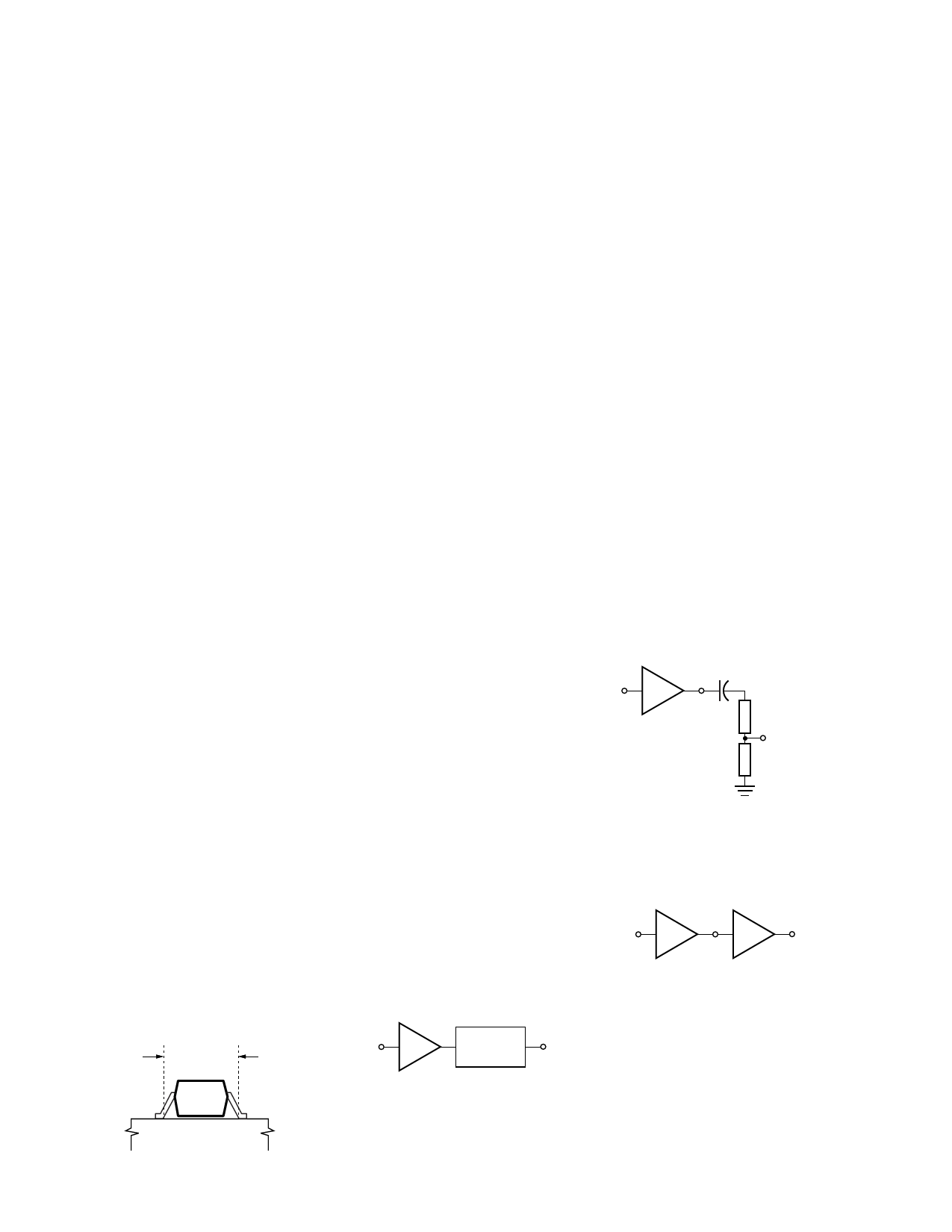
• A second implementation,
shown in Figure 11, uses a
simple reactive network at the
amplifier’s output to match the
output impedance to 50 Ω.
This matched output arrangement
will provide an additional 0.9 dB
of gain and output power at
900 MHz when driving into a 50 Ω
stage.
• The third way to use the INA-
30311 is to simply cascade
several INA-30311’s with 50 Ω
stages and neglect the effects of
the output mismatch.
The 50 Ω cascade without
impedance matching, shown in
Figure 12, trades off the
improvement in stage gain and
output power for a more
simplified interstage circuit and
reduced circuit board space.
INA-30
MATCHED
50 Ω OUTPUT
Figure 11. Impedance Matched
Output.
INA-30
50 Ω
INPUT
INA-30
HIGH Z
OUTPUT
Figure 12. Simple Cascade without
Impedance Matching.
TEST CIRCUIT
Figure 9. Reference Planes.
Figure 10. INA-30311 Driving a High
Input Impedance Stage.
6-143
Share Link: 