3083FE Ver la hoja de datos (PDF) - Linear Technology
Número de pieza
componentes Descripción
Fabricante
3083FE Datasheet PDF : 28 Pages
| |||
LT3083
APPLICATIONS INFORMATION
The LT3083 regulator is easy to use and has all the protection
features expected in high performance regulators. Included
are short-circuit protection and safe operating area protec-
tion, as well as thermal shutdown with hysteresis.
The LT3083 fits well in applications needing multiple rails.
This new architecture adjusts down to zero with a single
resistor, handling modern low voltage digital IC’s as well as
allowing easy parallel operation and thermal management
without heat sinks. Adjusting to zero output allows shutting
off the powered circuitry. When the input is pre-regulated,
such as with a 5V or 3.3V input supply, external resistors
can help spread the heat.
A precision “0” TC 50μA reference current source connects
to the noninverting input of a power operational amplifier.
The power operational amplifier provides a low impedance
buffered output to the voltage on the noninverting input.
A single resistor from the noninverting input to ground
sets the output voltage. If this resistor is set to 0Ω, zero
output voltage results. Therefore, any output voltage can
be obtained between zero and the maximum defined by
the input power supply.
The benefit of using a true internal current source as the
reference, as opposed to a bootstrapped reference in older
regulators, is not so obvious in this architecture. A true
reference current source allows the regulator to have gain
and frequency response independent of the impedance on
the positive input. On older adjustable regulators, such as
the LT1086, loop gain changes with output voltage and
bandwidth changes if the adjustment pin is bypassed to
ground. For the LT3083, the loop gain is unchanged with
output voltage changes or bypassing. Output regulation
is not a fixed percentage of output voltage, but is a fixed
fraction of millivolts. Use of a true current source allows
all of the gain in the buffer amplifier to provide regulation,
and none of that gain is needed to amplify up the reference
to a higher output voltage.
The LT3083 has the collector of the output transistor con-
nected to a separate pin from the control input. Since the
dropout on the collector (IN pin) is typically only 310mV,
two supplies can be used to power the LT3083 to reduce
dissipation: a higher voltage supply for the control circuitry
and a lower voltage supply for the collector. This increases
efficiency and reduces dissipation. To further spread the
heat, a resistor inserted in series with the collector moves
some of the heat out of the IC to spread it on the PC board
(see the section Reducing Power Dissipation).
The LT3083 can be operated in two modes. Three termi-
nal mode has the VCONTROL pin connected to the IN pin
and gives a limitation of 1.25V dropout. Alternatively, the
VCONTROL pin is separately tied to a higher voltage and the
IN pin to a lower voltage giving 310mV dropout on the IN
pin, minimizing total power dissipation. This allows for a
3A supply regulating from 2.5VIN to 1.8VOUT or 1.8VIN to
1.2VOUT with low power dissipation.
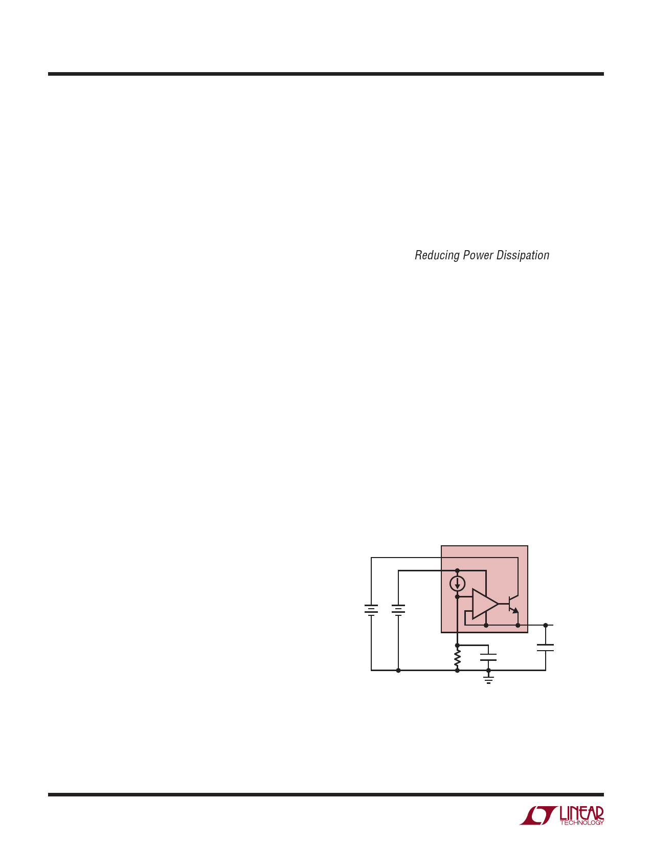
Programming Output Voltage
The LT3083 sources a 50μA reference current that flows
out of the SET pin. Connecting a resistor from SET to
ground generates a voltage that becomes the reference
point for the error amplifier (see Figure 1). The refer-
ence voltage equals 50µA multiplied by the value of
the SET pin resistor. Any voltage can be generated and
there is no minimum output voltage for the regulator.
IN
VCONTROL
++
VIN
VCONTROL
LT3083
50µA
+
–
SET
RSET
CSET
OUT
VOUT
COUT
3083 F01
VOUT = 50µA • RSET
Figure 1. Basic Adjustable Regulator
3083fa
10
Share Link: 