MPC7447A Ver la hoja de datos (PDF) - Freescale Semiconductor
Número de pieza
componentes Descripción
Fabricante
MPC7447A Datasheet PDF : 56 Pages
| |||
Electrical and Thermal Characteristics
Table 2. Absolute Maximum Ratings1 (continued)
Characteristic
Symbol Maximum Value Unit Notes
Storage temperature range
Tstg
–55 to 150
°C —
Notes:
1. Functional and tested operating conditions are given in Table 4. Absolute maximum ratings are stress ratings only, and
functional operation at the maximums is not guaranteed. Stresses beyond those listed may affect device reliability or cause
permanent damage to the device.
2. Caution: VDD/AVDD must not exceed OVDD by more than 1.0 V during normal operation; this limit may be exceeded for a
maximum of 20 ms during the power-on reset and power-down sequences.
3. Caution: OVDD must not exceed VDD/AVDD by more than 2.0 V during normal operation; this limit may be exceeded for a
maximum of 20 ms during the power-on reset and power-down sequences.
4. BVSEL must be set to 0, such that the bus is in 1.8-V mode.
5. BVSEL must be set to HRESET or 1, such that the bus is in 2.5-V mode.
6. Caution: Vin must not exceed OVDD by more than 0.3 V at any time including during power-on reset.
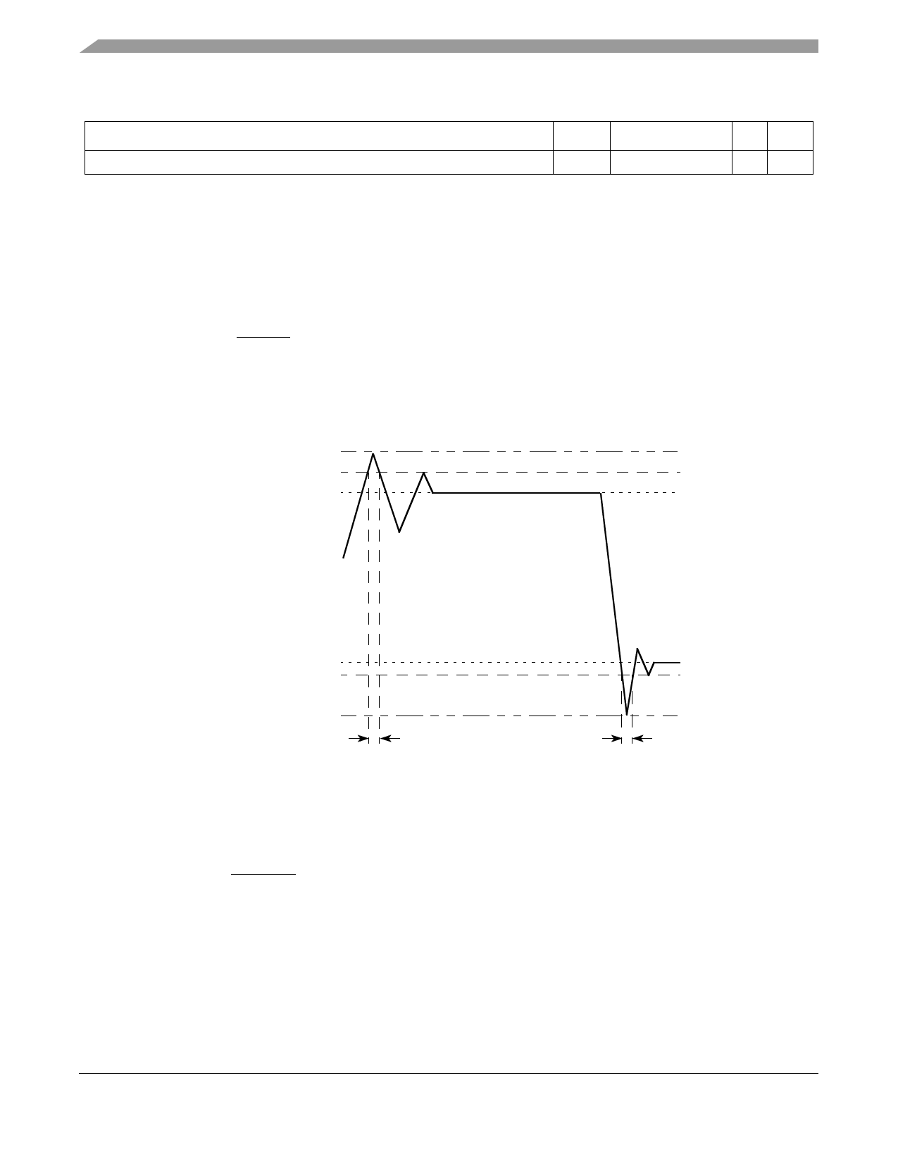
7. Vin may overshoot/undershoot to a voltage and for a maximum duration as shown in Figure 2.
Figure 2 shows the undershoot and overshoot voltage on the MPC7447A.
OVDD + 20%
OVDD + 5%
OVDD
VIH
VIL
GND
GND – 0.3 V
GND – 0.7 V
Not to Exceed 10%
of tSYSCLK
Figure 2. Overshoot/Undershoot Voltage
The MPC7447A provides several I/O voltages to support both compatibility with existing systems and
migration to future systems. The MPC7447A core voltage must always be provided at the nominal voltage
(see Table 4) or at the supported derated voltage (see Section 5.3, “Voltage and Frequency Derating”). The
input voltage threshold for each bus is selected by sampling the state of the voltage select pins at the
negation of the signal HRESET. The output voltage will swing from GND to the maximum voltage applied
to the OVDD power pins. Table 3 provides the input threshold voltage settings. Because these settings may
change in future products, it is recommended that BVSEL be configured using resistor options, jumpers,
or some other flexible means, with the capability to reconfigure the termination of this signal in the future
if necessary.
MPC7447A RISC Microprocessor Hardware Specifications, Rev. 5
10
Freescale Semiconductor
Share Link: 