IR2520 Ver la hoja de datos (PDF) - International Rectifier
Número de pieza
componentes Descripción
Fabricante
IR2520 Datasheet PDF : 17 Pages
| |||
IR2520D(S) & (PbF)
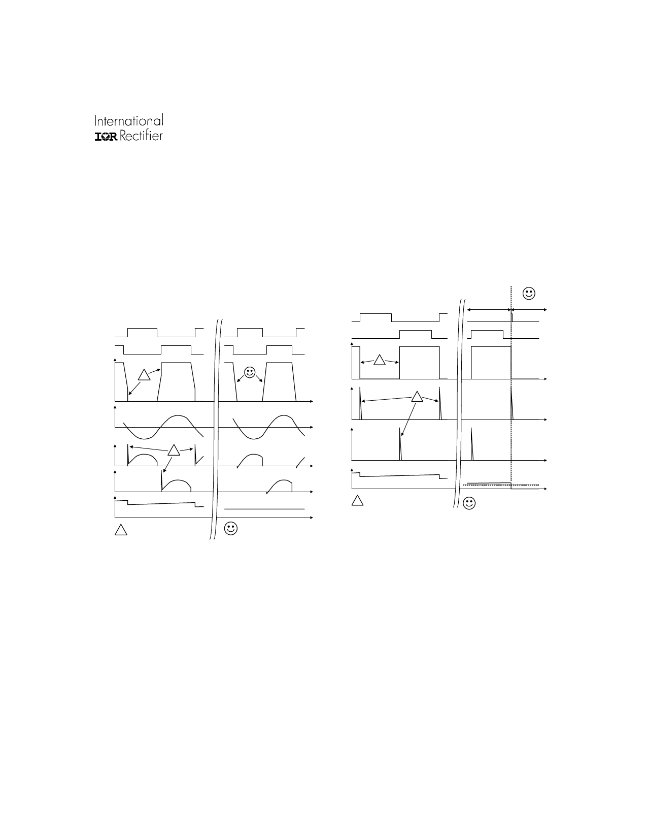
lamp removal (open circuit), a dropping DC bus during a
mains brown-out or mains interrupt, lamp variations over
time, or component variations. To protect against this, an
internal high-voltage MOSFET is turned on at the turn-off of
HO and the VS-sensing circuit measures VS at each rising
edge of LO. If the VS voltage is non-zero, a pulse of current
is sinked from the VCO pin (Figures 5 and 6) to slightly
discharge the external capacitor, CVCO, causing the
frequency to increase slightly. The VCO capacitor then
charges up during the rest of the cycle slowly due to the
internal current source.
VLO
VHO
VVS
!
IL
open circuit (Figure 7). This will cause capacitive switching
(hard-switching) resulting in high peak MOSFET currents
that can damage them. The IR2520D will increase the fre-
quency in attempt to satisfy ZVS until the VCO pin de-
creases below 0.82V (VVCOSD). The IC will enter Fault
Mode and latch the LO and HO gate driver outputs ‘low’ for
turning the half-bridge off safely before any damage can
occur to the MOSFETs.
VLO
VHO
VVS
!
RUN MODE FAULT MODE
!
IMLS
IMLS
!
IMHS
IMHS
VVCO
Too close to resonance.
! Hard-switching and high
peak MOSFET currents!
Frequency shifted higher
to maintain ZVS.
Fig. 6 IR2520D non-ZVS protection timing diagram.
VVCO
!
Capacitive switching. Hard-switching
and high peak MOSFET currents!
0.85V
Frequency shifted higher
until VCO < 0.82V. LO and
HO are latched low before
damage occurs to MOSFETs.
Fig. 7 Lamp removal or open filament fault
condition timing diagram
The frequency is trying to decrease towards resonance
by charging the VCO capacitor and the adaptive ZVS cir-
cuit “nudges” the frequency back up slightly above reso-
nance each time non-ZVS is detected at the turn-on of LO.
The internal high-voltage MOSFET is then turned off at the
turn-off of LO and it withstands the high-voltage when VS
slews up to the DC bus potential. The circuit then remains in
this closed-loop adaptive ZVS mode during running and
maintains ZVS operation with changing line conditions, com-
ponent tolerance variations and lamp/load variations. Dur-
ing a lamp removal or filament failure, the lamp resonant
tank will be interrupted causing the half-bridge output to go
Crest Factor Over-current Protection
During normal lamp ignition, the frequency sweeps through
resonance and the output voltage increases across the
resonant capacitor and lamp until the lamp ignites. If the
lamp fails to ignite, the resonant capacitor voltage, the inductor
voltage and inductor current will continue to increase until
the inductor saturates or the output voltage exceeds the
maximum voltage rating of the resonant capacitor or inductor.
The ballast must shutdown before damage occurs. To
protect against a lamp non-strike fault condition, the IR2520D
uses the VS-sensing circuitry (Figure 5) to also measure
the low-side half-bridge MOSFET current for detecting an
www.irf.com
9
Share Link: 