LV762102C Ver la hoja de datos (PDF) - SANYO -> Panasonic
Número de pieza
componentes Descripción
Fabricante
LV762102C Datasheet PDF : 6 Pages
| |||
LV762XXX Series
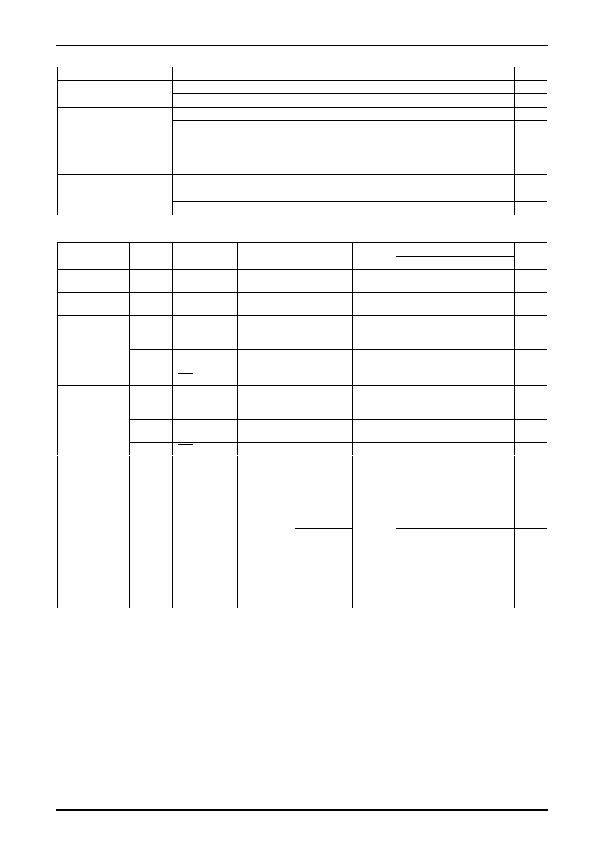
Operating Conditions (BIP Chip) at Ta = 25°C
Parameter
Recommended supply voltage
Recommended supply current
Operating supply voltage range
Operating supply current range
Symbol
V62
V4
I9
I20
I49
V62
V4
I9
I20
I49
Conditions
Ratings
Unit
5.0
V
5.0
V
11 mA
13 mA
22 mA
4.7 to 5.3
V
4.7 to 5.3
V
9 to 13 mA
11 to 15 mA
20.5 to 26.5 mA
Recommended Operating Range (Micro-computer Chip) at Ta = -10°C to +65°C, VSS = 0V
Parameter
Symbol
Pins
Conditions
VDD [V]
Ratings
min
typ
max
Operating supply
voltege
Hold voltage
High level input
voltage
Low level input
voltage
Operation cycle
time (*1)
Oscillation
frequency range
VDD
CpuVDD
0.229µs ≤ tCYC ≤ 200µs
4.5
VHD
VIH (1)
VIH (2)
VIH (3)
VIL (1)
VIL (2)
VIL (3)
tCYC (1)
tCYC (2)
FmVCO1
FmVCO1
(*2)
FmRC
CpuVDD
Ports0, 1,
P00 port input
/interrupt
Port00
Watch-dog timer
RES
Ports0, 1,
P00 port input
/interrupt
Port00
Watch-dog timer
RES
RAMs and the registers data are
kept in HOLD mode.
All functions operating
OSD and Data slicer are not
operating
Built-in VCO1
Oscillation System clock
Built-in VCO2 OCKSEL = 0
oscillation
OSD clock
OCKSEL = 1
Built-in RC oscillation
2.0
4.5 to 5.5
0.3VDD
+0.7
4.5 to 5.5 0.9VDD
4.5 to 5.5
4.5 to 5.5
0.75VDD
VSS
4.5 to 5.5
4.5 to 5.5
4.5 to 5.5
4.5 to 5.5
4.5 to 5.5
4.5 to 5.5
VSS
VSS
0.231
4.5 to 5.5
0.3
5.5
5.5
VDD
VDD
VDD
0.1VDD
+0.4
0.231
0.15VDD
+0.4
0.25VDD
200
13.0
12.5
16.6
1.0
2.0
FsX'tal
XT1 (P07)
At the 32.768KHz crystal
4.5 to 5.5
XT2 (P06)
Oscillating See the figure 1
Oscillation
tmsVCO
•after the HOLD mode
4.5 to 5.5
stabilizing time
•Power-On
(Note) FLASH-ROM erase/write temperature range : Ta = 25±2°C (VDD = 4.5 to 5.5V)
(*1) Relational expression between tCYC and oscillation frequency ;
1/1 frequency dividing : 3/FmVCO1, 1/2 frequency dividing : 6/FVCO1.
(*2) OCKSEL is the selectable register for OSD clock frequency. (See the LC873200 users manual for details.)
32.768
300
Unit
V
V
V
V
V
V
V
V
µs
µs
MHz
MHz
MHz
MHz
kHz
mS
No.A1447-3/6
Share Link: 