TA3020 Ver la hoja de datos (PDF) - Unspecified
Número de pieza
componentes Descripción
Fabricante
TA3020 Datasheet PDF : 27 Pages
| |||
Tripath Technology, Inc. - Technical Information
1/2 TA3020
V5
RFBA RFBA
Processing
&
Modulation
FBKOUT1
FBKGND1
RFBC
RFBC
OUT1
OUT 1 GROUND
RFBB RFBB
AGND
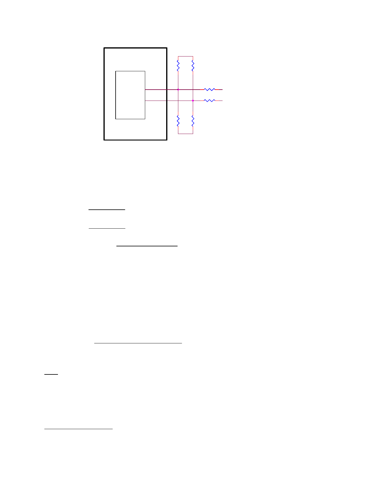
Figure 3: Modulator Feedback
The modulator feedback resistors are:
RFBA = User specified, typically 1K Ω
R FBB = RFBA * VPP
(VPP - 4)
R FBC = R FBA * VPP
4
A V - MODULATOR ≈ R FBC * (R FBA + R FBB ) + 1
R FBA * R FBB
The above equations assume that VPP=|VNN|.
For example, in a system with VPPMAX=52V and VNNMAX=-52V,
RFBA = 1kΩ, 1%
RFBB = 1.08kΩ, use 1.07kΩ, 1%
RFBC = 13.0kΩ, use 13.3kΩ, 1%
The resultant modulator gain is:
AV - MODULATOR ≈ 13.3k Ω * (1.0k Ω + 1.07k Ω ) + 1 = 26.73V/V
1.0k Ω * 1.07k Ω
Mute
When a logic high signal is supplied to MUTE, both amplifier channels are muted (both high- and low-side
transistors are turned off). When a logic level low is supplied to MUTE, both amplifiers are fully operational.
There is a delay of approximately 200 milliseconds between the de-assertion of MUTE and the un-muting of the
TA3020.
Turn-on & Turn-off Noise
If turn-on or turn-off noise is present in a TA3020 amplifier, the cause is frequently due to other circuitry
external to the TA3020. While the TA3020 has circuitry to suppress turn-on and turn-off transients, the
combination of the power supply and other audio circuitry with the TA3020 in a particular application may
18
TA3020 – KL Rev. 3.0/09.03
Share Link: 