TA3020 Ver la hoja de datos (PDF) - Unspecified
Número de pieza
componentes Descripción
Fabricante
TA3020 Datasheet PDF : 27 Pages
| |||
Tripath Technology, Inc. - Technical Information
R VNN1 = VNN
IVNNSENSE
Set R VNN2 = 3 × R VNN1 .
IVPPSENSE or IVNNSENSE can be any of the currents shown in the Electrical Characteristics table for
VPPSENSE and VNNSENSE, respectively.
The two resistors, RVPP2 and RVNN2 compensate for the internal bias points. Thus, RVPP1 and RVNN1 can be used
for the direct calculation of the actual VPP and VNN trip voltages without considering the effect of RVPP2 and
RVNN2.
Using the resistor values from above, the actual minimum over voltage turn off points will be:
VPP = R × I MIN_OV_TUR N_OFF
VPP1 VPPSENSE (MIN_OV_TU RN_OFF)
VNN = −(R × I ) MIN_OV_TUR N_OFF
VNN1 VNNSENSE (MIN_OV_TU RN_OFF)
The other three trip points can be calculated using the same formula but inserting the appropriate IVPPSENSE (or
IVNNSENSE) current value. As stated earlier, the usable supply range is the difference between the minimum
overvoltage turn off and maximum under voltage turn-off for both the VPP and VNN supplies.
VPP RANGE = VPP MIN_OV_TUR N_OFF - VPP MAX_UV_TUR N_OFF
VNN RANGE = VNN MIN_OV_TUR N_OFF - VNN MAX_UV_TUR N_OFF
VN10 Supply
VN10 is an additional supply voltage required by the TA3020. VN10 must be 10 volts more positive than the
nominal VNN. VN10 must track VNN. Generating the VN10 supply requires some care.
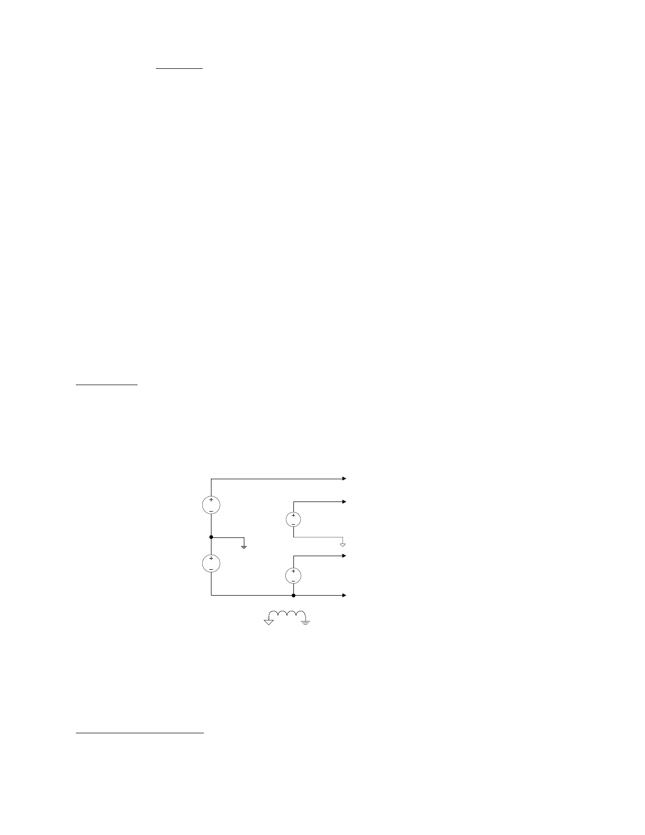
The proper way to generate the voltage for VN10 is to use a 10V-postive supply voltage referenced to the VNN
supply. Figure 5 shows the correct way to power the TA3020:
VPP
VNN
5V
PGND
10V
F. BEAD
VPP
V5
AGND
VN10
VNN
Figure 5: Proper Power Supply Connection
One apparent method to generate the VN10 supply voltage is to use a negative IC regulator to drop PGND
down to 10V (relative to VNN). This method will not work since negative regulators only sink current into the
regulator output and will not be capable of sourcing the current required by VN10. Furthermore, problems can
arise since VN10 will not track movements in VNN.
Output Transistor Selection
The key parameters to consider when selecting what MOSFET to use with the TA3020 are drain-source
breakdown voltage (BVdss), gate charge (Qg), and on-resistance (RDS(ON)).
21
TA3020 – KL Rev. 3.0/09.03
Share Link: 