EN5394QI Ver la hoja de datos (PDF) - Altera Corporation
Número de pieza
componentes Descripción
Fabricante
EN5394QI
Altera Corporation

EN5394QI Datasheet PDF : 19 Pages
| |||
The power supply has the following protection
features:
• Over-current protection with hiccup mode.
• Short Circuit protection.
• Thermal shutdown with hysteresis.
• Under-voltage lockout circuit to disable the
converter output when the input voltage is
less than approximately 2.2V
Enable Operation
The ENABLE pin provides a means to start
normal operation or to shut down the device. A
logic high will enable the converter into normal
operation. When the ENABLE pin is asserted
(high) the device will undergo a normal soft start.
A logic low will disable the converter. A logic low
will power down the device in a controlled
manner and the device is subsequently shut
down. The device will remain shut-down for the
duration of the ENABLE lockout time (see
Electrical Characteristics Table). If the ENABLE
signal is re-asserted during this time, the device
will power up with a normal soft-start at the end
of the ENABLE lockout time.
The Enable threshold is a precision Analog
voltage rather than a digital logic threshold.
Precision threshold along with choice of soft-start
capacitor helps to accurately sequence multiple
power supplies in a system.
Frequency Synchronization
The switching frequency of the DC/DC converter
can be phase-locked to an external clock source
to move unwanted beat frequencies out of band.
To avail this feature, the ternary input M/S pin
should be floating or pulled low. The internal
switching clock of the DC/DC converter can then
be phase locked to a clock signal applied to S_IN
pin. An activity detector recognizes the presence
of an external clock signal and automatically
phase-locks the internal oscillator to this external
clock. Phase-lock will occur as long as the input
clock frequency is within ±10% of the free
running frequency (see Electrical Characteristics
table). When no clock signal is present, the
device reverts to the free running frequency of
the internal oscillator. The external clock input
may be swept between 3.6 MHz and 4.4 MHz at
repetition rates of up to 10 kHz in order to reduce
EMI frequency components.
EN5394QI
Master / Slave Parallel Operation
Multiple EN5394QI devices may be connected in
parallel in a Master/Slave configuration to handle
load currents greater than device maximum
rating. The device is set in Master mode by
pulling the ternary M/S pin low or in Slave mode
by pulling M/S pin high to VIN through an external
resistor. When this pin is in Float state, parallel
operation is not possible. In master mode, the
internal PWM signal is output on the S_OUT pin.
This PWM signal from the Master can be fed to
one or more Slave devices at its S_IN input. The
Slave device acts like an extension of the power
FETs in the Master. As a practical matter,
paralleling more than 4 devices may be very
difficult from the view point of maintaining very
low impedance in VIN and VOUT lines.
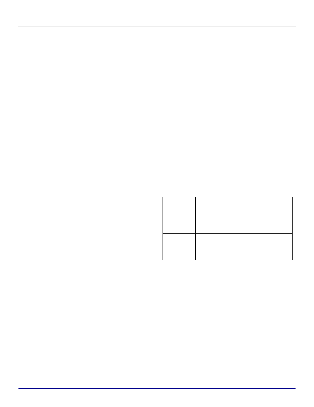
The table below summarizes the different
configurations for the S_IN and S_OUT pins
depending on the condition of the M/S pin:
When M/S High (Slave) Low (Master) Float
pin is:
S_IN input S_OUT from External Sync input if
should be: Master
needed (NC for internal
clock)
S_OUT is Same duty
equal to cycle as
(subject to S_IN
S_DELAY):
Same duty S_IN or
cycle as
internal
internal PWM clock
Please contact Altera Power Applications support
for more information on Master / Slave operation.
Phase Delay
In all cases, S_OUT can be delayed with respect
to internal switching clock or the clock applied to
S_IN. Multiple EN5394QI devices on a system
board may be daisy chained to reduce or
eliminate input ripple as well as avoiding beat
frequency components. The EN5394QIs can all
be phase locked by feeding S_OUT of one
device into S_IN of the next device in a daisy
chain. All the switchers now run at a common
frequency. The delay is controlled by the value of
a resistor connected between S_DELAY and
AGND pins. The magnitude of this delay as a
function of S_DELAY resistor is shown in the
03738
10
October 11, 2013
www.altera.com/enpirion
Rev E
Share Link: