AD7952 Ver la hoja de datos (PDF) - Analog Devices
NГғmero de pieza
componentes DescripciГіn
Fabricante
AD7952 Datasheet PDF : 32 Pages
| |||
AD7952
Data Sheet
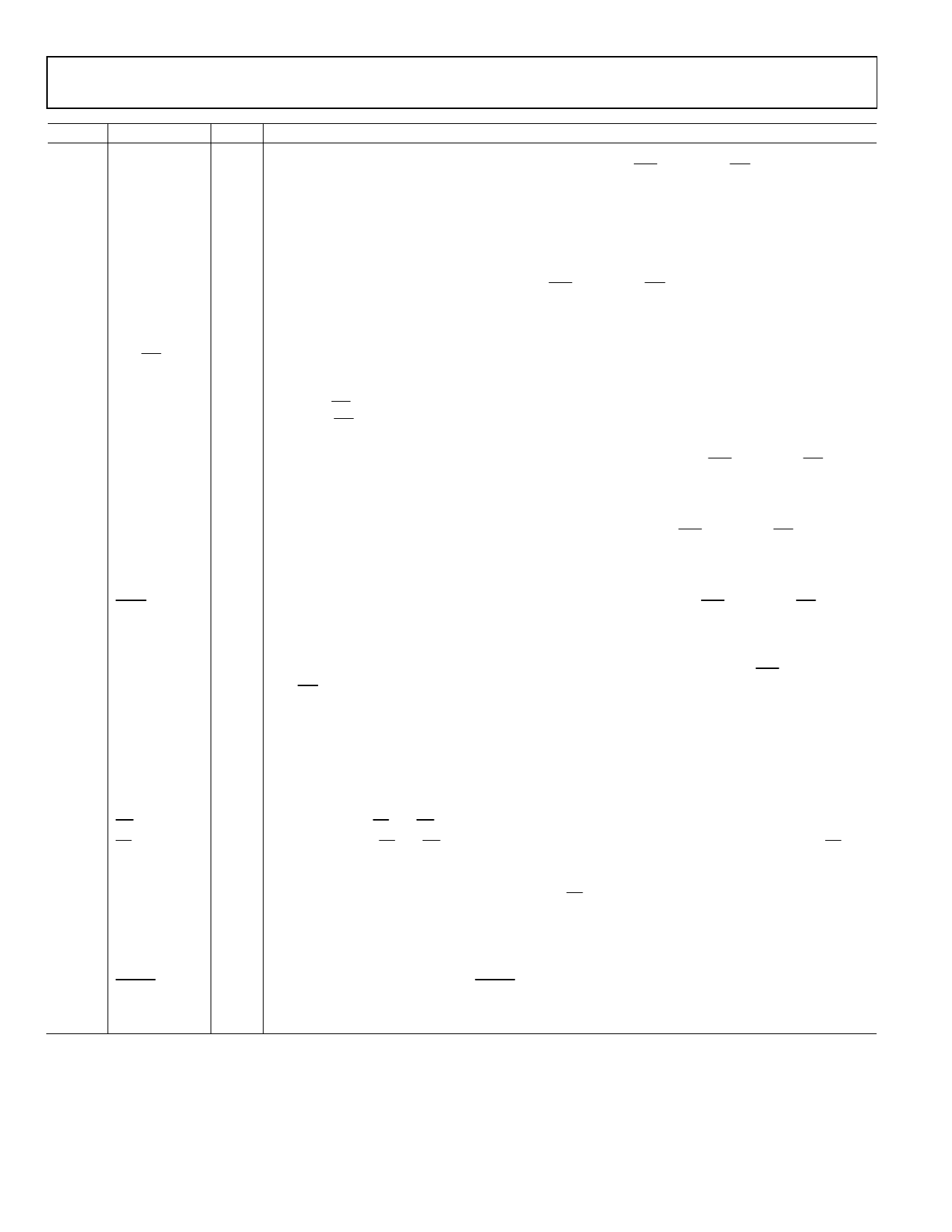
Pin No.
23
Mnemonic
D8 or
SYNC
24
D9 or
RDERROR
25
D10 or
HW/SW
26
D11 or
SCIN
27
D12 or
SCCLK
28
D13 or
SCCS
29
BUSY
30
TEN
31
RD
32
CS
33
RESET
34
PD
35
CNVST
36
BIPOLAR
Type1
DO
DO
DI/O
DI/O
DI/O
DI/O
DO
DI2
DI
DI
DI
DI2
DI
DI2
Description
In parallel mode, this output is used as Bit 8 of the parallel port data output bus.
Serial Data Frame Synchronization. In serial master mode (SER/PAR = high, EXT/INT= low), this
output is used as a digital output frame synchronization for use with the internal data clock.
When a read sequence is initiated and INVSYNC = low, SYNC is driven high and remains high while
the SDOUT output is valid.
When a read sequence is initiated and INVSYNC = high, SYNC is driven low and remains low while
the SDOUT output is valid.
In parallel mode, this output is used as Bit 9 of the parallel port data output bus.
Serial Data Read Error. In serial slave mode (SER/PAR = high, EXT/INT = high), this output is used as
an incomplete data read error flag. If a data read is started and not completed when the current
conversion is completed, the current data is lost and RDERROR is pulsed high.
In parallel mode, this output is used as Bit 10 of the parallel port data output bus.
Serial Configuration Hardware/Software Select. In serial mode, this input is used to configure
the AD7952 by hardware or software. See the Hardware Configuration section and Software
Configuration section.
When HW/SW = low, the AD7952 is configured through software using the serial configuration register.
When HW/SW = high, the AD7952 is configured through dedicated hardware input pins.
In parallel mode, this output is used as Bit 11 of the parallel port data output bus.
Serial Configuration Data Input. In serial software configuration mode (SER/PAR = high, HW/SW = low),
this input is used to serially write in, MSB first, the configuration data into the serial configuration
register. The data on this input is latched with SCCLK. See the Software Configuration section.
In parallel mode, this output is used as Bit 12 of the parallel port data output bus.
Serial Configuration Clock. In serial software configuration mode (SER/PAR = high, HW/SW = low), this
input is used to clock in the data on SCIN. The active edge where the data SCIN is updated depends
on the logic state of the INVSCLK pin. See the Software Configuration section.
In parallel mode, this output is used as Bit 13 of the parallel port data output bus.
Serial Configuration Chip Select. In serial software configuration mode (SER/PAR = high, HW/SW = low),
this input enables the serial configuration port. See the Software Configuration section.
Busy Output. Transitions high when a conversion is started and remains high until the conversion
is completed and the data is latched into the on-chip shift register. The falling edge of BUSY can be
used as a data-ready clock signal. Note that in master read after convert mode (SER/PAR = high,
EXT/INT = low, RDC = low), the busy time changes according to Table 4.
Input Range Select. Used in conjunction with BIPOLAR per the following.
Input Range (V)
BIPOLAR
TEN
0 to 5
Low
Low
0 to 10
Low
High
В±5
High
Low
В±10
High
High
Read Data. When CS and RD are both low, the interface parallel or serial output bus is enabled.
Chip Select. When CS and RD are both low, the interface parallel or serial output bus is enabled. CS
is also used to gate the external clock in slave serial mode (not used for serial configurable port).
Reset Input. When high, reset the AD7952. Current conversion, if any, is aborted. The falling edge of
RESET resets the data outputs to all zeros (with OB/2C = high) and clears the configuration register.
See the Digital Interface section. If not used, this pin can be tied to OGND.
Power-Down Input. When PD = high, powers down the ADC. Power consumption is reduced and
conversions are inhibited after the current one is completed. The digital interface remains active
during power-down.
Conversion Start. A falling edge on CNVST puts the internal sample-and-hold into the hold state and
initiates a conversion.
Input Range Select. See description for Pin 30.
Rev. A | Page 10 of 32
Share Link: 