AD5724R Ver la hoja de datos (PDF) - Analog Devices
Número de pieza
componentes Descripción
Fabricante
AD5724R
Analog Devices

AD5724R Datasheet PDF : 33 Pages
| |||
AD5724R/AD5734R/AD5754R
Data Sheet
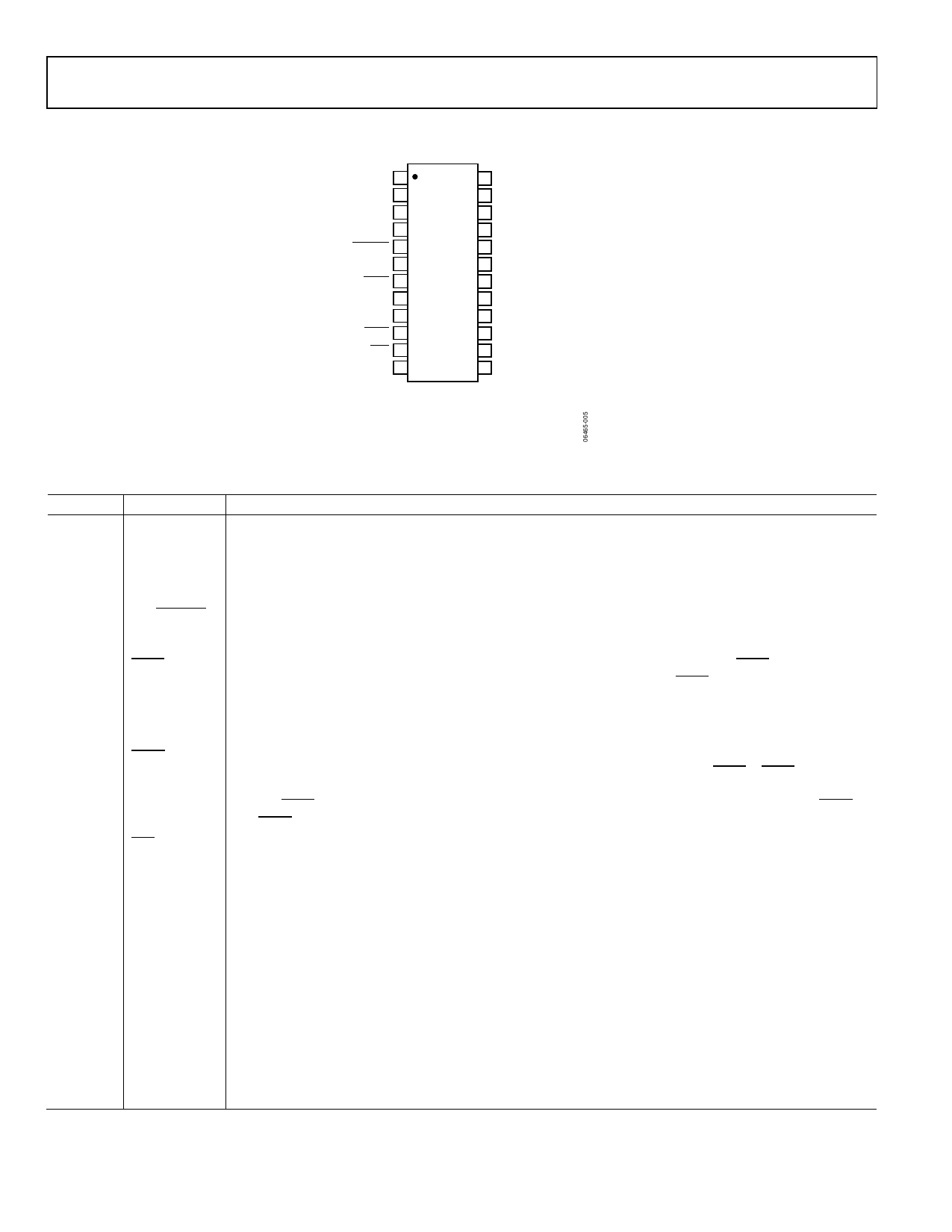
PIN CONFIGURATION AND FUNCTION DESCRIPTIONS
AVSS 1
24 AVDD
NC 2
23 VOUTC
VOUTA 3 AD5724R/ 22 VOUTD
VOUTB 4 AD5734R/ 21 SIG_GND
BIN/2sCOMP 5 AD5754R 20 SIG_GND
TOP VIEW
NC 6 (Not to Scale) 19 DAC_GND
SYNC 7
18 DAC_GND
SCLK 8
17 REFIN/REFOUT
SDIN 9
16 SDO
LDAC 10
15 GND
CLR 11
14 DVCC
NC 12
13 NC
NOTES
1. NC = NO CONNECT. DO NOT CONNECT TO THIS PIN.
2. IT IS RECOMMENDED THAT THE EXPOSED PAD BE
THERMALLY CONNECTED TO A COPPER PLANE
FOR ENHANCED THERMAL PERFORMANCE.
Figure 5. Pin Configuration
Table 6. Pin Function Descriptions
Pin No. Mnemonic
Description
1
AVSS
Negative Analog Supply Pin. Voltage range is from –4.5 V to –16.5 V. This pin can be connected to 0 V if
output ranges are unipolar.
2, 6, 12, 13 NC
No Connect. Do not connect to these pins.
3
VOUTA
Analog Output Voltage of DAC A. The output amplifier is capable of directly driving a 2 kΩ, 4000 pF load.
4
VOUTB
Analog Output Voltage of DAC B. The output amplifier is capable of directly driving a 2 kΩ, 4000 pF load.
5
BIN/2sCOMP This pin determines the DAC coding for a bipolar output range. This pin should be hardwired to either DVCC
or GND. When hardwired to DVCC, input coding is offset binary. When hardwired to GND, input coding is twos
complement. (For unipolar output ranges, coding is always straight binary.)
7
SYNC
Active Low Input. This is the frame synchronization signal for the serial interface. While SYNC is low, data is
transferred on the falling edge of SCLK. Data is latched on the rising edge of SYNC.
8
SCLK
Serial Clock Input. Data is clocked into the shift register on the falling edge of SCLK. This operates at clock
speeds up to 30 MHz.
9
SDIN
Serial Data Input. Data must be valid on the falling edge of SCLK.
10
LDAC
Load DAC, Logic Input. This is used to update the DAC registers and, consequently, the analog output. When
tied permanently low, the addressed DAC register is updated on the rising edge of SYNC. If LDAC is held high
during the write cycle, the DAC input register is updated, but the output update is held off until the falling
edge of LDAC. In this mode, all analog outputs can be updated simultaneously on the falling edge of LDAC.
The LDAC pin should not be left unconnected.
11
CLR
Active Low Input. Asserting this pin sets the DAC registers to zero-scale code or midscale code (user selectable).
14
DVCC
Digital Supply Pin. Voltage range is from 2.7 V to 5.5 V.
15
GND
Ground Reference Pin.
16
SDO
Serial Data Output. Used to clock data from the serial register in daisy-chain or readback mode. Data is
clocked out on the rising edge of SCLK and is valid on the falling edge of SCLK.
17
REFIN/REFOUT External Reference Voltage Input and Internal Reference Voltage Output. Reference input range is 2 V to 3 V.
REFIN = 2.5 V for specified performance. REFOUT = 2.5 V ± 2 mV at 25°C.
18, 19
DAC_GND
Ground reference pins for the four digital-to-analog converters.
20, 21
SIG_GND
Ground reference pins for the four output amplifiers.
22
VOUTD
Analog Output Voltage of DAC D. The output amplifier is capable of directly driving a 2 kΩ, 4000 pF load.
23
VOUTC
Analog Output Voltage of DAC C. The output amplifier is capable of directly driving a 2 kΩ, 4000 pF load.
24
AVDD
Positive Analog Supply Pin. Voltage range is from 4.5 V to 16.5 V.
EPAD
Exposed Paddle. The exposed paddle should be connected to the potential of the AVSS pin or, alternatively, it
can be left electrically unconnected. It is recommended that the paddle be thermally connected to a copper
plane for enhanced thermal performance.
Rev. G | Page 10 of 33
Share Link: