RJP30E2DPP-M0 Ver la hoja de datos (PDF) - Renesas Electronics
Número de pieza
componentes Descripción
Fabricante
RJP30E2DPP-M0
Renesas Electronics

RJP30E2DPP-M0 Datasheet PDF : 7 Pages
| |||
RJP30E2DPP-M0
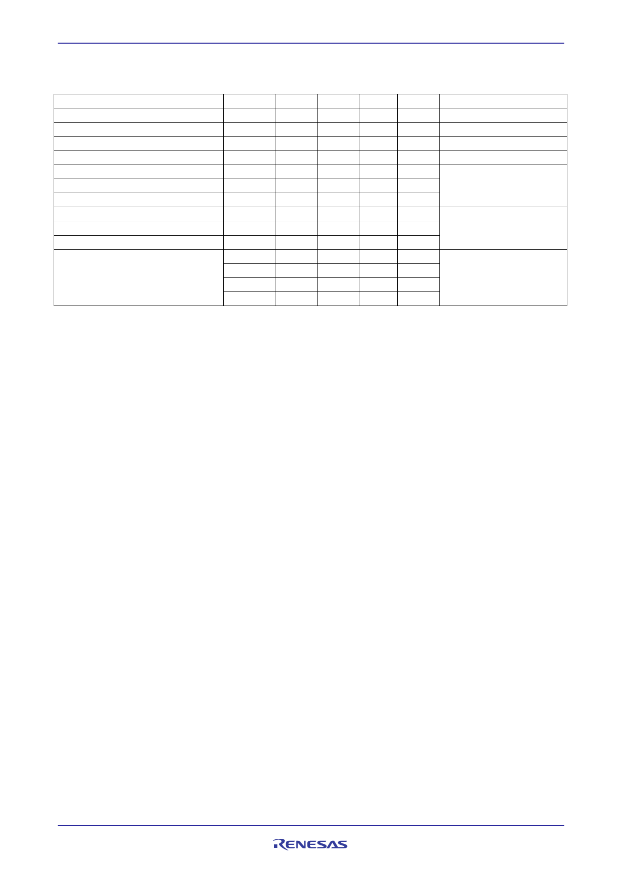
Electrical Characteristics
Item
Symbol Min
Zero gate voltage collector current
ICES
—
Gate to emitter leak current
IGES
—
Gate to emitter cutoff voltage
VGE(off)
2.5
Collector to emitter saturation voltage VCE(sat)
—
Input capacitance
Cies
—
Output capacitance
Coes
—
Reveres transfer capacitance
Cres
—
Total gate charge
Qg
—
Gate to emitter charge
Qge
—
Gate to collector charge
Qgc
—
Switching time
td(on)
—
tr
—
td(off)
—
tf
—
Notes: 3. Pulse test.
Preliminary
Typ
—
—
—
1.7
1160
60
26
34
6
10
0.03
0.1
0.08
0.15
Max
1
±100
5
2.2
—
—
—
—
—
—
—
—
—
—
Unit
μA
nA
V
V
pF
pF
pF
nC
nC
nC
μs
μs
μs
μs
(Ta = 25°C)
Test Conditions
VCE = 360 V, VGE = 0
VGE = ± 30 V, VCE = 0
VCE = 10 V, IC = 1 mA
IC = 35 A, VGE = 15 V Note3
VCE = 25 V
VGE = 0
f = 1 MHz
VGE = 15 V
VCE = 150 V
IC = 35 A
IC = 35 A
RL = 4.5 Ω
VGE = 15 V
RG = 5 Ω
R07DS0347EJ0200 Rev.2.00
Apr 12, 2011
Page 2 of 6
Share Link: