CY7C1318V18 Ver la hoja de datos (PDF) - Cypress Semiconductor
Número de pieza
componentes Descripción
Fabricante
CY7C1318V18 Datasheet PDF : 24 Pages
| |||
PRELIMINARY
CY7C1316V18
CY7C1318V18
CY7C1320V18
Maximum Ratings
Current into Outputs (LOW)......................................... 20 mA
(Above which the useful life may be impaired. For user guide-
lines, not tested.)
Storage Temperature .................................–65°C to +150°C
Static Discharge Voltage........................................... >2001V
(per MIL-STD-883, Method 3015)
Latch-up Current..................................................... >200 mA
Ambient Temperature with
Power Applied............................................. –55°C to +125°C
Supply Voltage on VDD Relative to GND........ –0.5V to +2.9V
DC Voltage Applied to Outputs
in High-Z State[12] ............................... –0.5V to VDDQ + 0.5V
DC Input Voltage[12] ............................ –0.5V to VDDQ + 0.5V
Operating Range
Range
Com’l
Ambient
Temperature[10]
0°C to +70°C
VDD
1.8 ± 100 mV
VDDQ
1.4V to VDD
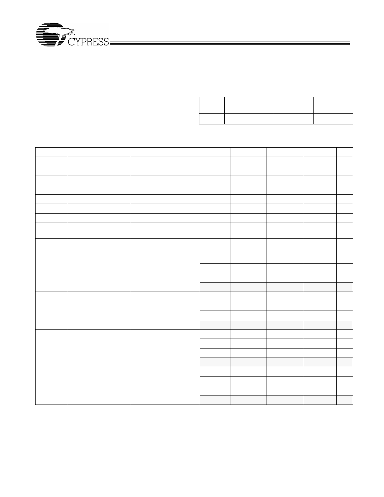
Electrical Characteristics Over the Operating Range[1, 11]
Parameter
Description
Test Conditions
Min.
Typ.
Max. Unit
VDD
VDDQ
VOH
VOL
VIH
VIL
IX
IOZ
VREF
Power Supply Voltage
I/O Supply Voltage
Output HIGH Voltage
Output LOW Voltage
Input HIGH Voltage[12]
Input LOW Voltage[12]
Input Load Current
Output Leakage
Current
Input Reference
Voltage[13]
IOH = −2.0 mA, Nominal Impedance
IOL = 2.0 mA, Nominal Impedance
GND ≤ VI ≤ VDDQ
GND ≤ VI ≤ VDDQ, Output Disabled
Typical Value = 0.75V
1.7
1.4
VDDQ – 0.2
VSS
VREF + 0.1
–0.3
–5
–5
1.8
1.9
V
1.5
VDD
V
VDDQ – 0.2
VDDQ
V
VSS
0.2
V
VREF + 0.1 VDDQ + 0.3 V
VREF – 0.1 VREF – 0.1 V
–5
5
µA
–5
5
µA
0.68
0.75
0.95
V
IDD
VDD Operating Supply VDD = Max., IOUT = 0 mA, 167 MHz
x8, x18
f = fMAX = 1/tCYC
200 MHz
250 MHz
TBD
mA
TBD
mA
TBD
mA
300 MHz
TBD
mA
IDD
VDD Operating Supply VDD = Max., IOUT = 0 mA, 167 MHz
x36
f = fMAX = 1/tCYC
200 MHz
TBD
mA
TBD
mA
250 MHz
TBD
mA
300 MHz
TBD
mA
ISB1
Automatic
Max. VDD, Both Ports
167 MHz
Power-down
Current, x8, x18
Deselected, VIN ≥ VIH or
VIN ≤ VIL f = fMAX = 1/tCYC,
200 MHz
Inputs Static
250 MHz
TBD
mA
TBD
mA
TBD
mA
300 MHz
TBD
mA
ISB1
Automatic
Power-down
Current, x36
Max. VDD, Both Ports
Deselected, VIN ≥ VIH or
VIN ≤ VIL f = fMAX = 1/tCYC,
Inputs Static
167 MHz
200 MHz
250 MHz
TBD
mA
TBD
mA
TBD
mA
300 MHz
TBD
mA
Notes:
10. Ambient temperature = TA. This is the case temperature.
11. All voltage referenced to ground.
12. Overshoot: VIH(AC) < VDD + 0.5V for t < tTCYC/2; undershoot VIL(AC) < − 0.5V for t < tTCYC/2; power-up: VIH < 1.8V and VDD < 1.8V and VDDQ < 1.4V for
t < 200 ms.
13. VREF Min. = 0.68V or 0.46VDDQ, whichever is larger, VREF Max. = 0.95V or 0.54VDDQ, whichever is smaller.
Document #: 38-05177 Rev. *A
Page 10 of 24
Share Link: 