QHX220 Ver la hoja de datos (PDF) - Intersil
Número de pieza
componentes Descripción
Fabricante
QHX220 Datasheet PDF : 19 Pages
| |||
QHx220
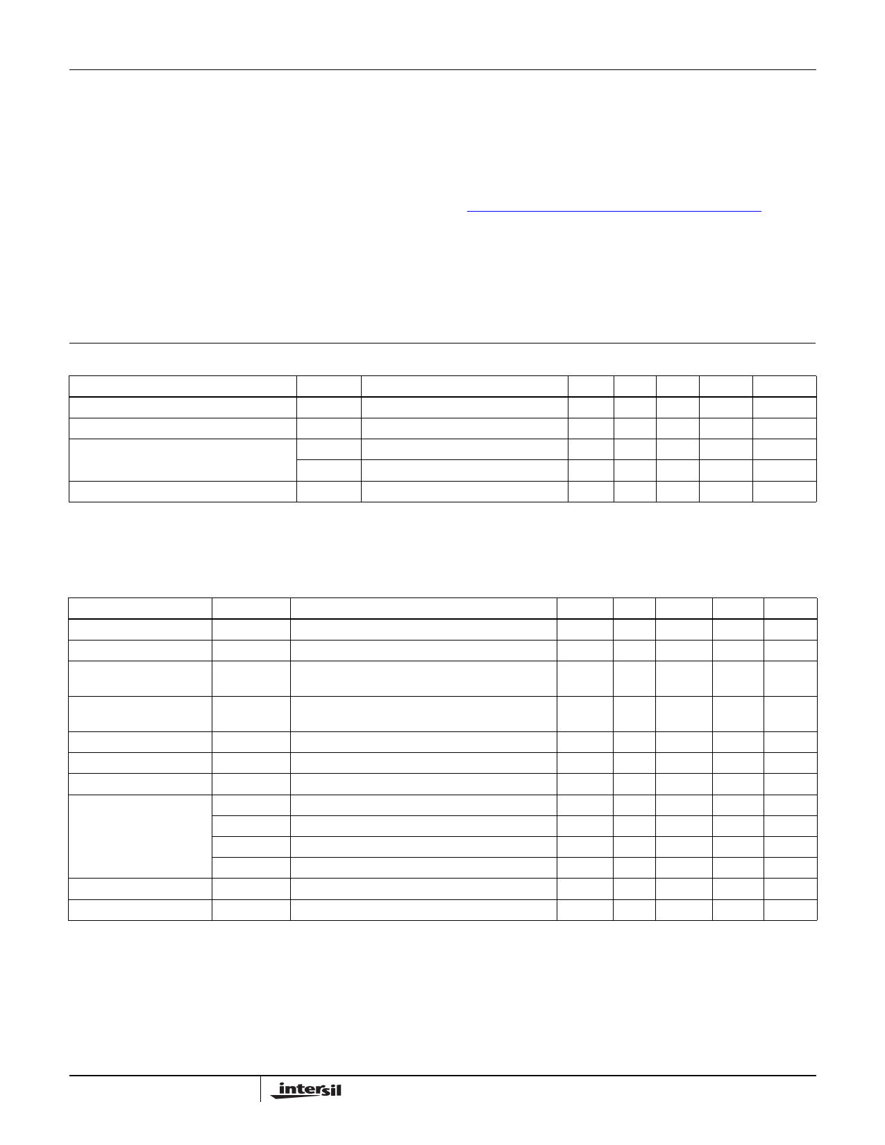
Absolute Maximum Ratings
Supply Voltage (VDD to GND) . . . . . . . . . . . . . . . . . . .2.1V
I/O Voltage at All Input Pins . . . . GND - 0.3V to VDD + 0.3V
ESD Rating (HBM) . . . . . . . . . . . . . . . . . . . . . . . . . . . 2kV
Thermal Information
Thermal Resistance (Typical)
θJA (°C/W) θJC (°C/W)
16 Ld QFN Package (Notes 3, 4) . .
60
13
Operating Ambient Temperature Range . . . . -40°C to +85°C
Storage Ambient Temperature Range . . . . -55°C to +150°C
Maximum Junction Temperature . . . . . . . . . . . . . . . +125°C
Pb-free reflow profile . . . . . . . . . . . . . . . . . . .see link below
http://www.intersil.com/pbfree/Pb-FreeReflow.asp
CAUTION: Do not operate at or near the maximum ratings listed for extended periods of time. Exposure to such conditions may adversely impact
product reliability and result in failures not covered by warranty.
NOTES:
3. θJA is measured with the component mounted on a high effective thermal conductivity test board in free air. See Tech Brief
TB379 for details.
4. For θJC, the “case temp” location is the center of the exposed metal pad on the package underside.
Operating Conditions
PARAMETER
SYMBOL
CONDITION
Supply Voltage
Operating Ambient Temperature
Power Consumption (operation mode)
VDD
TA
@high/low gain mode
@boost gain mode
Power Consumption (standby mode)
NOTE:
5. Max Power specifications tested under ECC test conditions.
MIN
1.7
-40
TYP
1.8
25
16
23
10
MAX UNITS
1.9
V
85
°C
28.7 mW
33 mW
38.3 µW
NOTES
5
5
5
Control Pin Characteristics Typical values are at VDD = 1.8V, TA = +25°C, and PIN = < -48dBm, unless otherwise noted.
Extreme Characterization Conditions (ECC) are VDD = 1.7V to 1.9V, TA = -40°C to +85°C.
PARAMETER
SYMBOL
CONDITION
MIN TYP MAX UNITS NOTES
Logic Input Level - Low ENBAR low
0.2 VDD mV
Logic Input Level - High ENBAR high
0.8 VDD
V
Enable Response Time
Delay following high to low transition until RF
535
output is within 10% of its final value.
ns
6
Disable Response Time
Delay following low to high transition until RF
350
ns
output is within 10% of its final value.
Control Word Length
24
Bits
Bits 0-9
I-DAC value
10
Bits
Bits 10-19
Q-DAC value
10
Bits
Bits 20-21
Application select
00: UHF-Band
01: L-Band
11: ISM Band
Bit 22
Gain Switch
1
Bit
Bit 23 (Note 18)
Extended Feature
1
Bit
7
NOTES:
6. The enable response time is bounded by the input AC cap on board. Typical response time reflects 100pF capacitance.
7. Generally set to low. Two successive SPI instructions are needed to enable or disable boost gain mode.
Sequence to enable boost gain mode → 1st instruction: set Bit<23:20> to 1x01’b
→ 2nd instruction: set Bit<23:20> to 0xxx’b
Sequence to disable boost gain mode → 1st instruction: set Bit<23:20> to 1x10’b
→ 2nd instruction: set Bit<23:20> to 0xxx’b
4
FN6986.0
October 20, 2009
Share Link: 