MAX691AD Ver la hoja de datos (PDF) - Maxim Integrated
Número de pieza
componentes Descripción
Fabricante
MAX691AD Datasheet PDF : 16 Pages
| |||
Microprocessor Supervisory Circuits
Table 1. Reset Pulse Width and Watchdog Timeout Selections
OSC SEL
Low
Low
Floating
Floating
OSC IN
External Clock Input
External Capacitor
Low
Floating
Watchdog Timeout Period
Normal
Immediately After Reset
1024 clks
4096 clks
(600/47pF x C)ms
(2.4/47pF x C)sec
100ms
1.6sec
1.6sec
1.6sec
Reset Timeout Period
2048 clks
(1200/47pF x C)ms
200ms
200ms
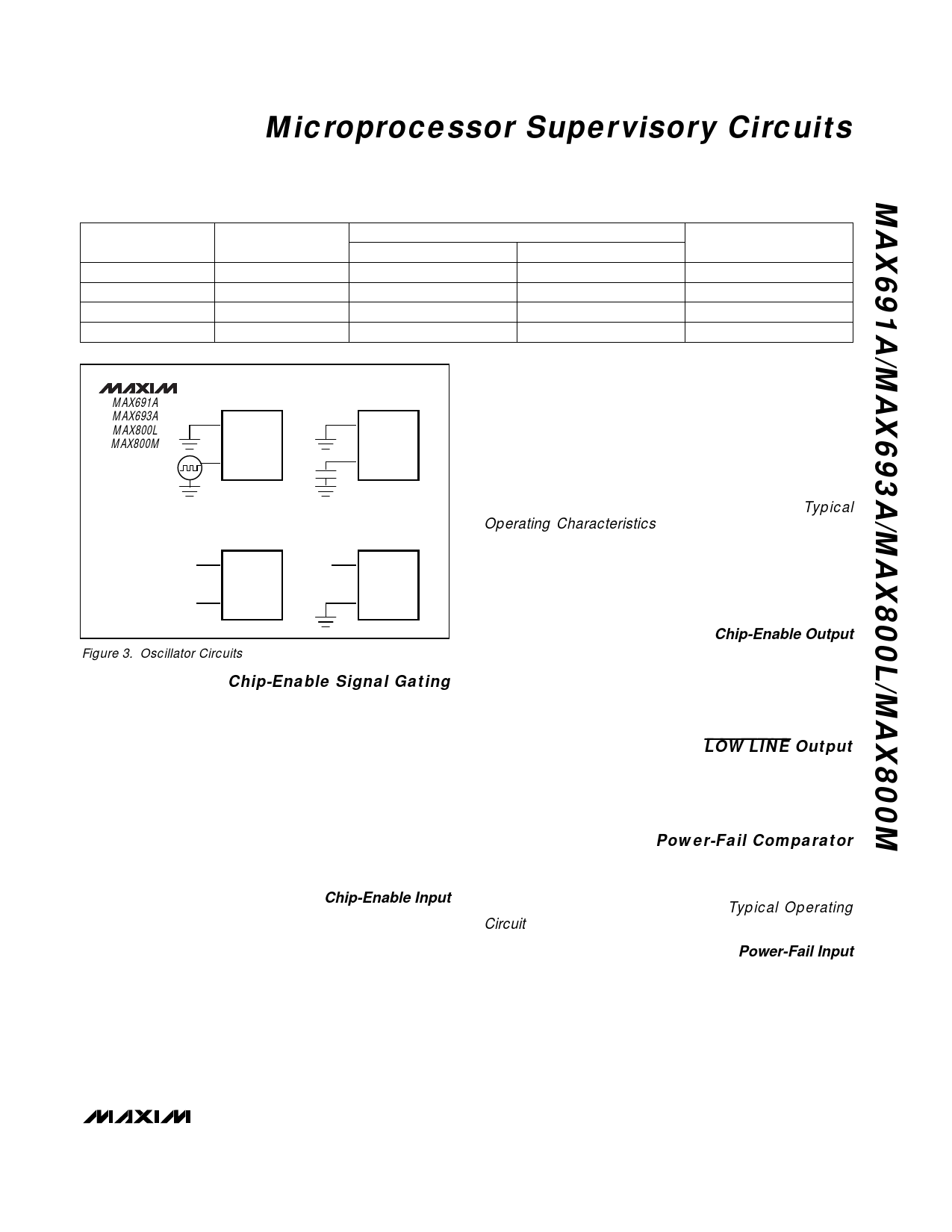
MAX691A
MAX693A
MAX800L
MAX800M
50kHz
EXTERNAL
CLOCK
8 OSC SEL
7 OSC IN
EXTERNAL
OSCILLATOR
8 OSC SEL
7 OSC IN
INTERNAL OSCILLATOR
1.6sec WATCHDOG
INTERNAL OSCILLATOR
100ms WATCHDOG
N.C. 8 OSC SEL
N.C. 8 OSC SEL
N.C. 7 OSC IN
7 OSC IN
Figure 3. Oscillator Circuits
Chip-Enable Signal Gating
The MAX691A/MAX693A/MAX800L/MAX800M provide
internal gating of chip-enable (CE) signals to prevent
erroneous data from being written to CMOS RAM in the
event of a power failure. During normal operation, the
CE gate is enabled and passes all CE transitions. When
reset is asserted, this path becomes disabled, prevent-
ing erroneous data from
these parts use a series
tcraonrrsumpitsinsgionthgeaCteMfOroSmRC–AEMI.NAtoll
CE OUT (Figure 4).
The 10ns max CE propagation delay from CE IN to CE
OUT enables the parts to be used with most µPs.
Chip-Enable Input
aTbheledChmipo-dEen)awbhleileInRpEuSt E(CTEanINd)R–—isE—Sh—Ei—gT–haimrepaesdsaenrtceed.(dis-
atDhuehriirngeghs-eaitmpthporewedseahr-ondlcdoewosnr taasetweqauwtcehhnedcneogtwhfheaeurvleto, lVC–taCEgCIeNfaaalltsss–CbuEemloeINws
goes high or 15µs after reset is asserted, whichever
occurs first (Figure 5).
During a power-up sequence, CE IN remains high
impedance, regardless of CE IN activity, until reset is
deasserted following the reset timeout period.
In the high-impedance mode, the leakage currents into
tlohwis-itmeprmedinaanlcaerem±od1eµ,Athmeaimx poevdear ntceemopfeC–raEtuINre.apIpnetahres
as a 75Ω resistor in series with the load at CE OUT.
The propagation delay through the CE transmission
gate
drive
dtoep–CeEnIdNs
Enable Output
on
(a–CnEd
both the source impedance of the
the capacitive loading on the Chip-
OUT) (see Chip-Enable Propagation
Delay vs. CE OUT Load Capacitance in the Typical
i5Os0pp%erroapdtoiunicngttioConfha–CterEastceOtdeUrifTsrotiumcssi)nt.hgeTa5h0e5%0CΩpEodpirnrivot eporaf agC–naEdtioIN5n0tdpoeFtlhaoeyf
load capacitance (Figure 6). For minimum propagation
delay, minimize the capacitive load at CE OUT, and
use a low output-impedance driver.
Chip-Enable Output
In the enabled mode, the impedance of CE OUT is
equivalent to 75Ω in series with the source driving CE
IN. In the disabled mode, the 75Ω transmission gate is
off and CE OUT is actively pulled to VOUT. This source
turns off when the transmission gate is enabled.
L–—O—W——L——IN—E– Output
LOW LINE is the buffered output of the reset threshold
comparator. LOW LINE typically sinks 3.2mA at 0.1V.
For normal operation (VCC above the LOW LINE thresh-
old), LOW LINE is pulled to VOUT.
Power-Fail Comparator
The power-fail comparator is an uncommitted comparator
that has no effect on the other functions of the IC.
Common uses include low-battery indication (Figure 7),
and early power-fail warning (see Typical Operating
Circuit).
Power-Fail Input
Power Fail Input (PFI) is the input to the power-fail com-
parator. It has a guaranteed input leakage of ±25nA
max over temperature. The typical comparator delay is
25µs from VIL to VOL (power failing), and 60µs from VIH
to VOH (power being restored). If PFI is not used, con-
nect it to ground.
_______________________________________________________________________________________ 9
Share Link: 