HT45FM03B Ver la hoja de datos (PDF) - Holtek Semiconductor
Número de pieza
componentes Descripción
Fabricante
HT45FM03B Datasheet PDF : 83 Pages
| |||
HT45FM03B
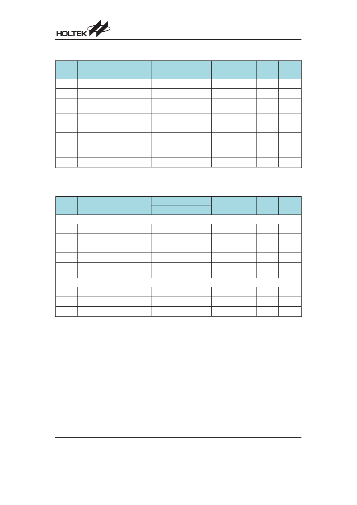
A/D Converter Characteristics
Symbol
Parameter
Test Conditions
VDD
Conditions
AVDD A/D Converter Operating Voltage ¾
¾
VAD AD Input Voltage
¾
¾
VREF
A/D Converter Input Reference
Voltage Range
¾
¾
DNL Differential Non-linearity
¾ tAD= 0.5ms
INL
Integral Non-linearity
¾ tAD= 0.5ms
IADC
Additional Power Consumption if
A/D Converter is Used
5V No load, tAD= 0.5ms
tAD
A/D Converter Clock Period
¾
¾
tADC
A/D Conversion Time (Note)
¾ 12 bit ADC
Note: ADC conversion time (tADC) is include ADC sample time 4tAD.
Min.
4.5
0
¾
¾
¾
¾
0.5
¾
OP Amplifier Electrical Characteristics
Symbol
Parameter
D.C. Electrical Characteristic
VDD
Operating Voltage
VOS
Input Offset Voltage
VCM
Common Mode Voltage Range
PSRR Power Supply Rejection Ratio
CMRR Common Mode Rejection Ratio
A.C. Electrical Characteristic
AOL
Open Loop Gain
SR
Slew Rate+, Rate-
GBW Gain Band Width
Test Conditions
VDD
Conditions
¾
¾
5V By calibration
¾
¾
¾
¾
¾
VDD=5V
VCM=0~VDD-1.4V
¾
¾
¾ No load
¾ RL=1MW, CL=100pF
Min.
4.5
-5
VSS
60
60
60
¾
¾
Ta=25°C
Typ. Max. Unit
¾
VDD
V
¾
VREF
V
AVDD
¾
V
±1
±2
LSB
±2
±4
LSB
1.5
3.0
mA
¾
100
ms
16
¾
tAD
Ta=25°C
Typ. Max. Unit
¾
5.5
V
¾
5
mV
¾
VDD-1.4
V
¾
¾
dB
¾
¾
dB
80
¾
dB
1
¾
V/ms
¾
100
kHz
Rev. 1.10
8
May 7, 2010
Share Link: 