D8255 Ver la hoja de datos (PDF) - Digital Core Design
Número de pieza
componentes Descripción
Fabricante
D8255 Datasheet PDF : 4 Pages
| |||
KEY FEATURES
● Compatible with industry standard 8255
● 24 I/O lines individually programmed in
2 groups of 12:
○ Group A - Port A and upper half of Port C
○ Group B – Port B and lower half of Port C
● 3 major modes of operation
○ Mode 0 – Basic input/output
○ Mode 1 – Strobed Input/output
○ Mode 2 – Bi-directional Bus
● Control Word Read-Back Capability
● Direct Bit Set/Reset Capability
● Interrupt control functions
● No internal three states busses
● Fully synthesizable technology independ-
ent source code.
DESIGN FEATURES
♦ ONE GLOBAL SYSTEM CLOCK
♦ SYNCHRONOUS RESET
♦ ALL ASYNCHRONOUS INPUT SIGNALS ARE
SYNCHRONIZED BEFORE INTERNAL USE
♦ ALL LATCHES IMPLEMENTED IN ORIGINAL
8255 DEVICES ARE REPLACED BY EQUIVA-
LENT FLIP-FLOP REGISTERS, WITH THE SAME
FUNCTIONALITY
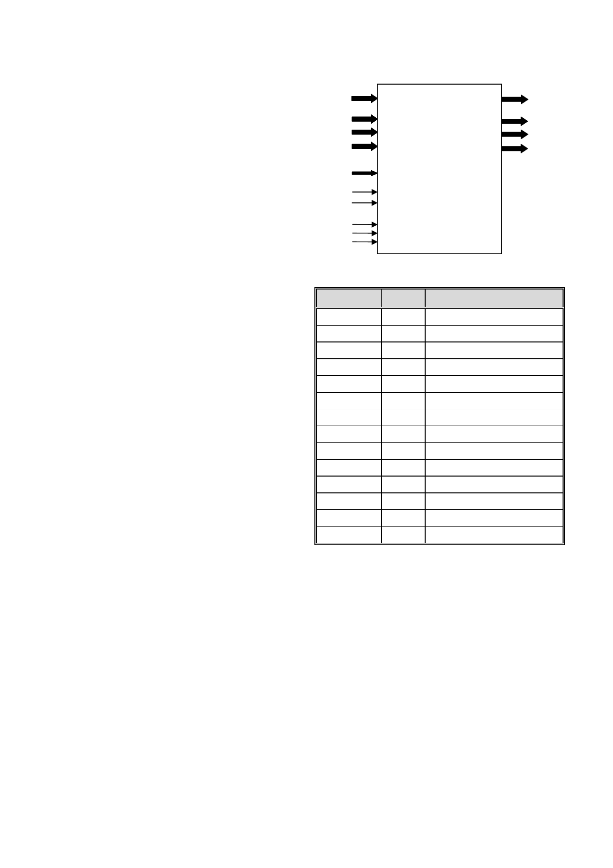
SYMBOL
datai(7:0)
portai(7:0)
portbi(7:0)
portci(7:0)
datao (7:0)
portao (7:0)
portbo (7:0)
portco (7:0)
a(1:0)
we
rd
cs
rst
clk
PINS DESCRIPTION
PIN
clk
reset
cs
rd
we
a[1:0]
portai[7:0]
portbi[7:0]
portci[7:0]
datai[7:0]
datao[7:0]
portao[7:0]
portbo[7:0]
portco[7:0]
TYPE
DESCRIPTION
input Global clock
input Global reset
input Chip select
input Processor read strobe
input Processor write strobe
input Processor address lines
input Port A input
input Port B input
input Port C input
input Data bus (input)
output Data bus (output)
output Port A output
output Port B output
output Port C output
APPLICATIONS
● Embedded microprocessor boards
● Interface to the printer
● I/O component to interface peripheral
● equipment to the microcomputer system
bus
All trademarks mentioned in this document
are trademarks of their respective owners.
BLOCK DIAGRAM
Data Bus Buffer– The Data Bus Buffer is
used to interface the D8255 to the system
data bus. Data is transmitted or received by
the buffer upon execution of input or output
instructions by the CPU. Control words and
status information are also transferred
through the data bus buffer.
Read/Write and Control Logic - The control
logic block manages all of the internal and
external transfers of both Data and Control or
Status words. It accepts inputs from the CPU
Address and Control busses and in turn, is-
sues commands to both of the Control
Groups A and B.
http://www.DigitalCoreDesign.com
http://www.dcd.pl
Copyright 1999-2007 DCD – Digital Core Design. All Rights Reserved.
Share Link: 