BH15LB1WG Ver la hoja de datos (PDF) - ROHM Semiconductor
Número de pieza
componentes Descripción
Fabricante
BH15LB1WG Datasheet PDF : 9 Pages
| |||
BH □□FB1WG series, BH□□FB1WHFV series,
BH □□LB1WG series, BH□□LB1WHFV series, BH □□MA3WHFV series
Technical Note
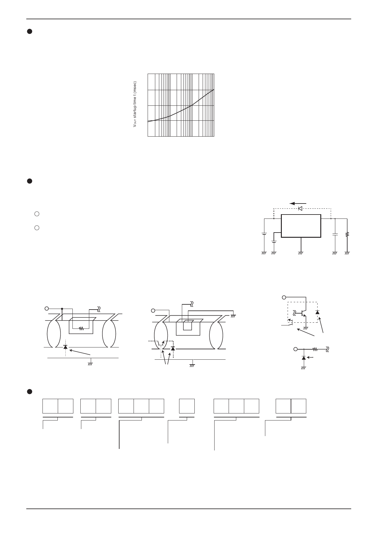
Noise terminal (BHŜŜMA3WHFV)
The terminal is directly connected to inward normal voltage source. Because this has low current ability, load exceeding
100nA will cause some instability at the output. For such reasons, we urge you to use ceramic capacitors which have less
leak current. When choosing noise the current reduction capacitor, there is a trade-off between boot-up time and stability. A
bigger capacitor value will result in lesser oscillation but longer boot-up time for VOU T.
100
BH30MA3WHFV
~ Condition ~
VIN=4.0V
10
Cin=1.0μF
Co=1.0μF
ROUT=3.0kΩ
1
Ta=25°C
0.1
0.01
100P
1000P
0.01μ
0.1μ
noise-filtering capacitor capacitance Cn (F)
Fig. 35: V OUT startup time vs. noise-filtering capacitor capacitance characteristics (Example)
Regarding input pin of the IC
This monolithi c IC contains P+ isolation and P substrat e layer s between adjacent
elements in order to keep them isolated. P/N junctions are formed at the intersection of
these P layers with the N layers of other elements to create a variety of parasitic elements.
For example, when a resistor and transistor are connected to pins as shown in Fig.37
The P/N junction functions as a parasitic diode when GND > (Pin A) for the resistor or
GND > (Pin B) for the transistor (NPN).
Similarly, when GND > (Pin B) for the transistor (NPN), the parasitic diode described
above combines with the N layer of other adjacent elements to operate as a parasitic
NPN transistor.
The formation of parasitic elements as a result of the relationships of the potentials of
different pins is an inevitable result of the IC's architecture. The operation of parasitic
elements can cause interference with circuit operation as well as IC malfunction and
damage. For these reasons, it is necessary to use caution so that the IC is not used in a
way that will trigger the operation of parasitic elements, such as by the application of
voltage lower than the GND (P substrate) voltage to input pins.
back current
VCC
OUT
CTL
GND
Fig. 36: Example of bypass
diode connection
(Terminal A)
Resistor
P+
N
P
P
N
P+
N
P-board
Parasitic element
GND
(Terminal B)
O
Transistor (NPN)
B
E
P+
N
N
P
N
P
Parasitic elements
GND
Fig.37
GND
P+
N
(Terminal B)
C
B
E
Other adjacent elements
GND
Parasitic elements
(Terminal A)
Parasitic element
GND
Part number selection
BH 3 0 FB1 W HFV - TR
ROHM
Output
part number voltage
Current capacity
MA3 : 300mA
FB1 : 150mA
LB1 : 150mA
Shutdown
switch
W : With switch
Package
HFV : HVSOF6
HVSOF5
G : SSOP5
Package specification
TR : Embossed taping
www.rohm.com
© 2010 ROHM Co., Ltd. All rights reserved.
7/8
2010.07 - Rev. C
Share Link: 