M28C17 Ver la hoja de datos (PDF) - STMicroelectronics
Número de pieza
componentes Descripción
Fabricante
M28C17 Datasheet PDF : 17 Pages
| |||
M28C17
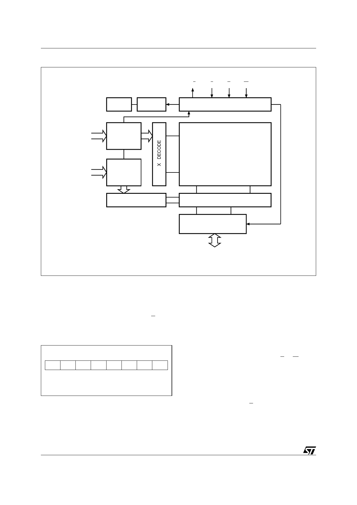
Figure 3. Block Diagram
VPP GEN
RESET
A6-A10
(Page Address)
ADDRESS
LATCH
A0-A5
ADDRESS
LATCH
Y DECODE
RB
E
G
W
CONTROL LOGIC
64K ARRAY
SENSE AND DATA LATCH
I/O BUFFERS
DQ0-DQ7
PAGE LOAD
TIMER STATUS
TOGGLE BIT
DATA POLLING
AI01488
Microcontroller Control Interface
The M28C17 provides two write operation status
bits and one status pin that can be used to minimize
the system write cycle. These signals are available
on the I/O port bits DQ7 or DQ6 of the memory
during programming cycle only, or as the RB signal
on a separate pin.
Figure 4. Status Bit Assignment
DQ7 DQ6 DQ5 DQ4 DQ3 DQ2 DQ1 DQ0
DP TB PLTS Hi-Z Hi-Z Hi-Z Hi-Z Hi-Z
DP = Data Polling
TB = Toggle Bit
PLTS = Page Load Timer Status
Data Polling bit (DQ7). During the internal write
cycle, any attempt to read the last byte written will
produce on DQ7 the complementary value of the
previously latched bit. Once the write cycle is fin-
ished the true logic value appears on DQ7 in the
read cycle.
Toggle bit (DQ6). The M28C17 offers another way
for determining when the internal write cycle is
completed. During the internal Erase/Write cycle,
DQ6 will toggle from "0" to "1" and "1" to "0" (the
first read value is "0") on subsequent attempts to
read the memory. When the internal cycle is com-
pleted the toggling will stop and the device will be
accessible for a new Read or Write operation.
Page Load Timer Status bit (DQ5). In the Page
Write mode data may be latched by E or W. Up to
64 bytes may be input. The Data output (DQ5)
indicates the status of the internal Page Load
Timer. DQ5 may be read by asserting Output En-
able Low (tPLTS). DQ5 Low indicates the timer is
running, High indicates time-out after which the
write cycle will start and no new data may be input.
Ready/Busy pin. The RB pin provides a signal at
its open drain output which is low during the
erase/write cycle, but which is released at the
completion of the programming cycle.
4/17
Share Link: 