Z53C80 Ver la hoja de datos (PDF) - Zilog
Número de pieza
componentes Descripción
Fabricante
Z53C80 Datasheet PDF : 40 Pages
| |||
ZILOG
FUNCTIONAL DESCRIPTION (Continued)
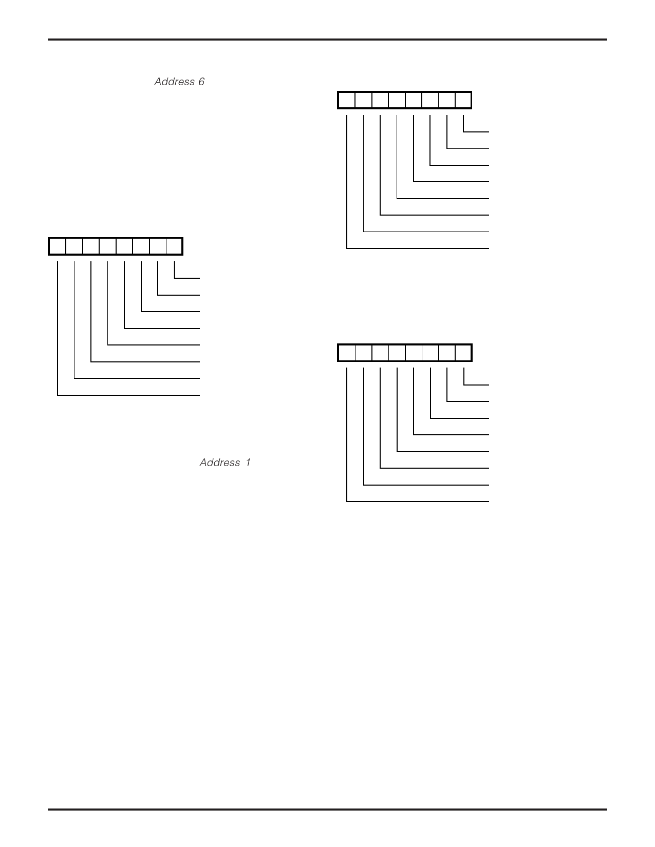
Input Data Register. Address 6 (Read Only). The input
Data Register (Figure 7) is a read-only register that is used
to read latched data from the SCSI Bus. Data is latched
either during a DMA Target receive operation when /ACK
goes active or during a DMA Initiator receive when /REQ
goes active. The DMA Mode bit (Mode Register bit 1) must
be set before data can be latched in the Input Data
Register. This register is read under DMA control using
/RD and /DACK. Parity is optionally checked when the
Input Data Register is loaded.
Address: 1
(Read Only)
D7 D6 D5 D4 D3 D2 D1 D0
Address: 6
(Read Only)
D7 D6 D5 D4 D3 D2 D1 D0
Z53C80 SCSI
Assert Data Bus
Assert /ATN
Assert /SEL
Assert /BSY
Assert /ACK
Lost Arbitration
Arbitration in Progress
Assert /RST
/DB0
/DB1
/DB2
/DB3
/DB4
/DB5
/DB6
/DB7
Figure 7. Input Data Register
Initiator Command Register. Address 1 (Read/Write).
The Initiator Command Register (Figures 8 and 9) are read
and write registers which assert certain SCSI Bus signals,
monitors those signals, and monitors the progress of bus
arbitration. Many of these bits are significant only when
being used as an Initiator; however, most can be used
during Target role operation.
Figure 8. Initiator Command Register
(Register Read)
Address: 1
(Write Only)
D7 D6 D5 D4 D3 D2 D1 D0
Assert Data Bus
Assert /ATN
Assert /SEL
Assert /BSY
Assert /ACK
"0"
Test Mode
Assert /RST
Figure 9. Initiator Command Register
(Register Write)
8
PS97SCC0200
Share Link: 