WED2ZL361MS42BI Ver la hoja de datos (PDF) - White Electronic Designs Corporation
Número de pieza
componentes Descripción
Fabricante
WED2ZL361MS42BI Datasheet PDF : 12 Pages
| |||
White Electronic Designs
WED2ZL361MS
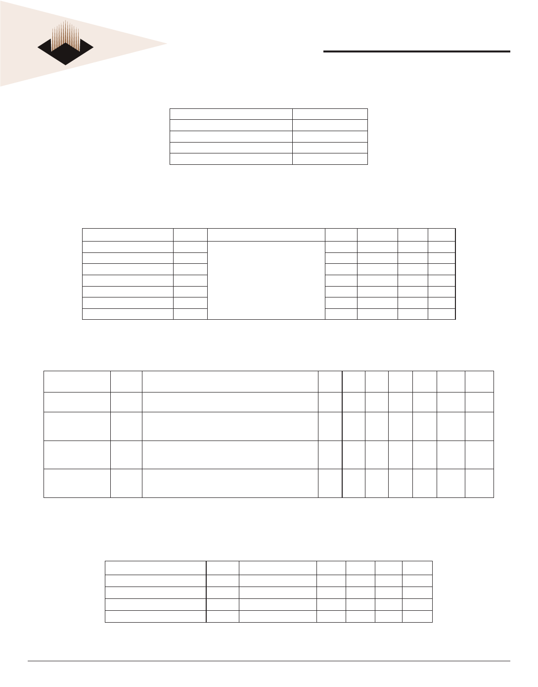
ABSOLUTE MAXIMUM RATINGS*
Voltage on VCC Supply Relative to VSS
Vin (DQx)
Vin (Inputs)
Storage Temperature (BGA)
Short Circuit Output Current
-0.3V to +3.6V
-0.3V to +3.6V
-0.3V to +3.6V
-55°C to +125°C
100mA
*Stress greater than those listed under “Absolute Maximum Ratings: may cause permanent damage to the device. This is a stress rating
only and functional operation of the device at these or any other conditions greater than those indicated in the operational sections of this
specification is not implied. Exposure to absolute maximum rating condtions for extended periods may affect reliability.
RECOMMENDED DC OPERATING CONDITIONS
(Voltage Referenced to: VSS = OV, TA = 0°C; Commercial or -40°C ≤ TA ≤ 85°C; Industrial)
Description
Input High (Logic 1) Voltage
Input Low (Logic 0) Voltage
Input Leakage Current
Output Leakage Current
Output High Voltage
Output Low Voltage
Supply Voltage
Symbol
VIH
VIL
ILI
ILO
VOH
VOL
VCC
Conditions
0V ≤ VIN ≤ VCC
Output(s) Disabled, 0V ≤ VIN ≤ VCC
IOH = -1.0mA
IOL = 1.0mA
Min
1.7
-0.3
-5
-5
2.0
–
2.375
NOTES:
1. All voltages referenced to VSS (GND)
2. ZZ pin has an internal pull-up, and input leakage is higher.
DC CHARACTERISTICS
Max
VCC +0.3
0.7
5
5
–
0.4
2.625
Units
V
V
µA
µA
V
V
V
Notes
1
1
2
1
1
1
Description
Symbol
Conditions
Power Supply
Current: Operating
IDD
Device Selected; All Inputs � VIL or � VIH; Cycle
Time = TCYC MIN; VCC = MAX; Output Open
Power Supply
Current: Standby
ISB2
Power Supply
Current: Current
ISB3
Device Deselected; VCC = MAX; All Inputs� VSS + 0.2
or VCC - 0.2; All Inputs Static; CK Frequency = 0;
ZZ � VIL
Device Selected; All Inputs � VIL or � VIH; Cycle
Time = TCYC MIN; VCC = MAX; Output Open;
ZZ � VCC - 0.2V
Clock Running
Standby Current
ISB4
Device Deselected; VCC = MAX; All Inputs
� VSS + 0.2 or VCC - 0.2; Cycle Time = TCYC
MIN; ZZ � VIL
NOTES:
1. IDD is specified with no output current and increases with faster cycle times.
IDD increases with faster cycle times and greater output loading.
2. Typical values are measured at 2.5V, 25°C, and 10ns cycle time.
Typ
250
MHz
200
MHz
166
MHz
133
MHz
Units
Notes
900 800 690 580 mA
1, 2
30 60 60 60
60
mA
2
20 40 40 40
40
mA
2
150 140 130 100 mA
2
BGA CAPACITANCE
Description
Symbol
Conditions
Typ Max Units Notes
Control Input Capacitance
CI
TA = 25°C; f = 1MHZ
5
7
pF
1
Input/Output Capacitance (DQ) CO
TA = 25°C; f = 1MHZ
6
8
pF
1
Address Capacitance
CA
TA = 25°C; f = 1MHZ
5
7
pF
1
Clock Capacitance
CCK
TA = 25°C; f = 1MHZ
3
5
pF
1
NOTES:
1. This parameter is sampled.
White Electronic Designs Corp. reserves the right to change products or specifications without notice.
Oct, 2002
Rev. 5
4
White Electronic Designs Corporation • (602) 437-1520 • www.wedc.com
Share Link: 