US1150 Ver la hoja de datos (PDF) - Unisem
Número de pieza
componentes Descripción
Fabricante
US1150 Datasheet PDF : 5 Pages
| |||
US1150
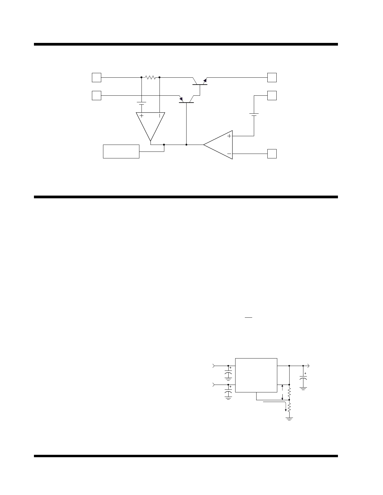
BLOCK DIAGRAM
Vin
Vctrl
+
CURRENT
LIMIT
1.25V +
THERMAL
SHUTDOWN
1150blk1-1.1
Figure 1 - Simplified block diagram of the US1150
Vout
Vsense
Adj
APPLICATION INFORMATION
Introduction
The US1150 adjustable regulator is a 5 terminal device
designed specificaly to provide extremely low dropout
voltages comparable to the PNP type without the disad-
vantage of the extra power dissipation due to the base
current associated with PNP regulators.This is done by
bringinging out the control pin of the regulator that pro-
vides the base current to the power NPN and connect-
ing it to a voltage that is grater than the voltage present
at the Vin pin.This flexebility makes the US1150 ideal
for applications where dual inputs are available such as
a computer motherboard with an ATX style power sup-
ply that provides 5V and 3.3V to the board.One such
application is the new graphic chip sets that require any-
where from 2.4V to 2.7V supply such as the Intel I740
chip set. The US1150 can easily be programmed with
the addition of two external resistors to any voltages
within the range of 1.25 to 5.5 V. Another major require-
ment of these graphic chips such as the Intel I740 is the
need to switch the load current from zero to several amps
in tens of nanoseconds at the processor pins ,which
translates to an approximately 300 to 500 nS of current
step at the regulator . In addition, the output voltage tol-
erances are also extremely tight and they include the
transient response as part of the specification.
The US1150 is specifically designed to meet the fast
current transient needs as well as providing an accurate
initial voltage , reducing the overall system cost with the
need for fewer number of output capacitors.Another fea-
ture of the device is its true remote sensing capability
which allows accurate voltage setting at the load rather
than at the device.
Output Voltage Setting
The US1150 can be programmed to any voltages in the
range of 1.25V to 5.5V with the addition of R1 and R2
external resistors according to the following formula:
VOUT
=
VREF1+
R2
R1
+ IADJ
× R2
Wehre : VREF=1.25V Typically
IADJ=50 uA Typically
R1 & R2 as shown in figure 2
Vin
Vctrl
Vin
Vout
US1150
Vctrl
Vsense
Adj
Vref R1
Vout
IAdj = 50uA R2
1150app2-1.1
Figure 2 - Typical application of the US1150 for
programming the output voltage.
2-4
Rev. 1.2
10/28/99
Share Link: 