HV3137PG Ver la hoja de datos (PDF) - Supertex Inc
Número de pieza
componentes Descripción
Fabricante
HV3137PG Datasheet PDF : 5 Pages
| |||
HV3137
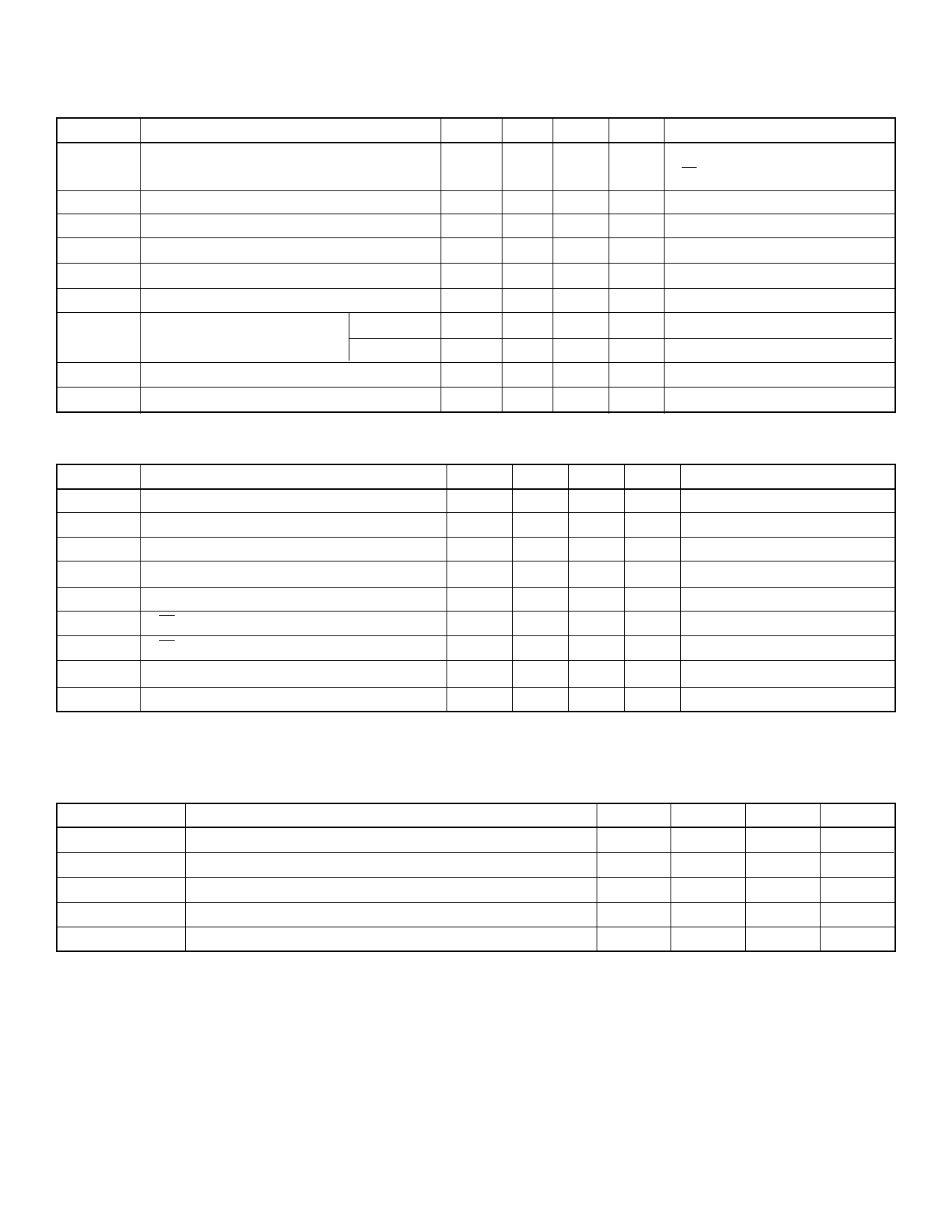
Electrical Characteristics (over recommended operating conditions unless noted)
DC Characteristics
Symbol
IDD
IDDQ
IO(OFF)
IIH
IIL
VOH
VOL
VOC
CHVO
Parameter
VDD Supply Current
Min Typ
Quiescent VDD Supply Current
Off State Output Current at 25°C, per Switch
High-Level Logic Input Current
Low-Level Logic Input Current
High-Level Data Out
Low-Level Output
HVOUT
Data Out
VDD -1V
HVOUT Clamp Voltage
Output Capacitance per Channel
Max Units
15
mA
250
µA
100
nA
10
µA
-10
µA
V
10
V
1
V
-3.0
V
3
pF
Conditions
fCLK = 6MHz, fDATA = 3MHz
LE = LOW
All VIN = 0V
Output high, and at 375V
VIH = VDD
VI = 0V
IDOUT = -100µA
IHVOUT = +1mA
IDOUT = +100µA
IOL = -1mA
VDS = 100V
AC Characteristics
Symbol
fCLK
tW
tSU
tH
tWLE
tDLE
tSLE
tDHL
tDLH
Parameter
Clock Frequency
Clock Width High or Low
Data Setup Time Before Clock Falls
Data Hold Time After Clock Falls
Width of Latch Enable Pulse
LE Delay Time After Falling Edge of Clock
LE Setup Time Before Falling Edge of Clock
Clock Delay Time Data High to Low
Clock Delay Time Data Low to High
Min Typ Max Units
6
MHz
83
ns
35
ns
15
ns
83
ns
35
ns
40
ns
135
ns
135
ns
Conditions
Recommended Operating Conditions
Symbol
Parameter
VDD
Logic supply voltage
HVOUT
High voltage output
VIH
High-level input voltage
VIL
Low-level input voltage
TA
Operating free-air temperature
Notes:
Power-up sequence should be the following:
1. Connect ground.
2. Apply VDD.
3. Set all inputs (Data, CLK, Enable, etc.) to a known state.
4. Apply VPP.
Power-down sequence should be the reverse of the above.
Min
Typ
Max
Units
4.5
5
5.5
V
8.0
375
V
3.5
VDD
V
0
0.8
V
-40
+85
°C
2
Share Link: 