NT7701H Ver la hoja de datos (PDF) - Novatek Microelectronics
Número de pieza
componentes Descripción
Fabricante
NT7701H Datasheet PDF : 37 Pages
| |||
NT7701
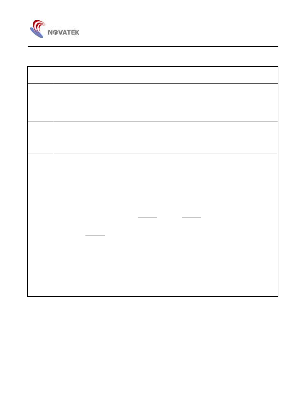
Pad Description
Segment mode
Symbol
Function
VDD
Logic system power supply pin connects to +2.5 to +5.5V
VSS
Ground pin connects to 0V
VOR, VOL
V12R, V12L
V43R, V43L
V5R, V5L
Power supply pin for LCD driver voltage bias
# Normally, the bias voltage used is set by a resistor divider
# Ensure that the voltages are set such that VSS ≤ V5 < V43 < V12 < V0
# To further reduce the differences between the output waveforms of the LCD driver output pins Y1 and Y160,
externally connect ViR and ViL (I = 0, 12, 43)
D0 - D7
Input pin for display data
# In 4-bit parallel input mode, input data into the 4 pins D0 - D3. Connect D4 - D7 to VSS or VDD
# In 8-bit parallel input mode, input data into the 8 pins D0 - D7
XCK
Clock input pin for taking display data
# Data is read on the falling edge of the clock pulse
LP
Latch pulse input pin for display data
# Data is latched on the falling edge of the clock pulse
Direction selection pin for reading display data
L/R
# When set to VSS level "L", data is read sequentially from Y160 to Y1
# When set to VDD level "H", data is read sequentially from Y1 to Y160
DISPOFF
Control input pin for output deselect level
# The input signal is level-shifted from logic voltage level to LCD driver voltage level, and controls LCD
driver circuit
# When set to VSS level “L”, the LCD driver output pins (Y1 - Yl60) are set to level V5
# While DISPOFF is set to “L”, the contents of the line latch are reset, but the display data in the data latch
are read regardless of the condition of DISPOFF . When the DISPOFF function is canceled, the driver
outputs deselect level (V12 or V43), then outputs the contents of the date latch onto the next falling edge
of the LP.
That time, if DISPOFF removal time can not keep regulation what is shown AC characteristics, can not
output the reading data correctly
AC signal input for LCD driving waveform
# The input signal is level-shifted from the logic voltage level to the driver voltage level, and controls LCD
FR
driver circuit
# Normally inputs a frame inversion signal
The LCD driver output pin’s output voltage level can be set to the line latch output signal and the FR signal
Mode selection pin
MD
# When set to VSS level “L”, 4-bit parallel input mode is set
# When set to VDD level “H", 8-bit parallel input mode is set
7
Share Link: 