TCL1117 Ver la hoja de datos (PDF) - TelCom Semiconductor, Inc
Número de pieza
componentes Descripción
Fabricante
TCL1117
TelCom Semiconductor, Inc

TCL1117 Datasheet PDF : 9 Pages
| |||
PRELIMINARY INFORMATION
TCL1117
TCL1117-2.85
TCL1117-3.30
TCL1117-5.00
800mA LOW DROPOUT POSITIVE REGULATORS
ADJUSTABLE AND FIXED 2.85V, 3.30V, 5.00V
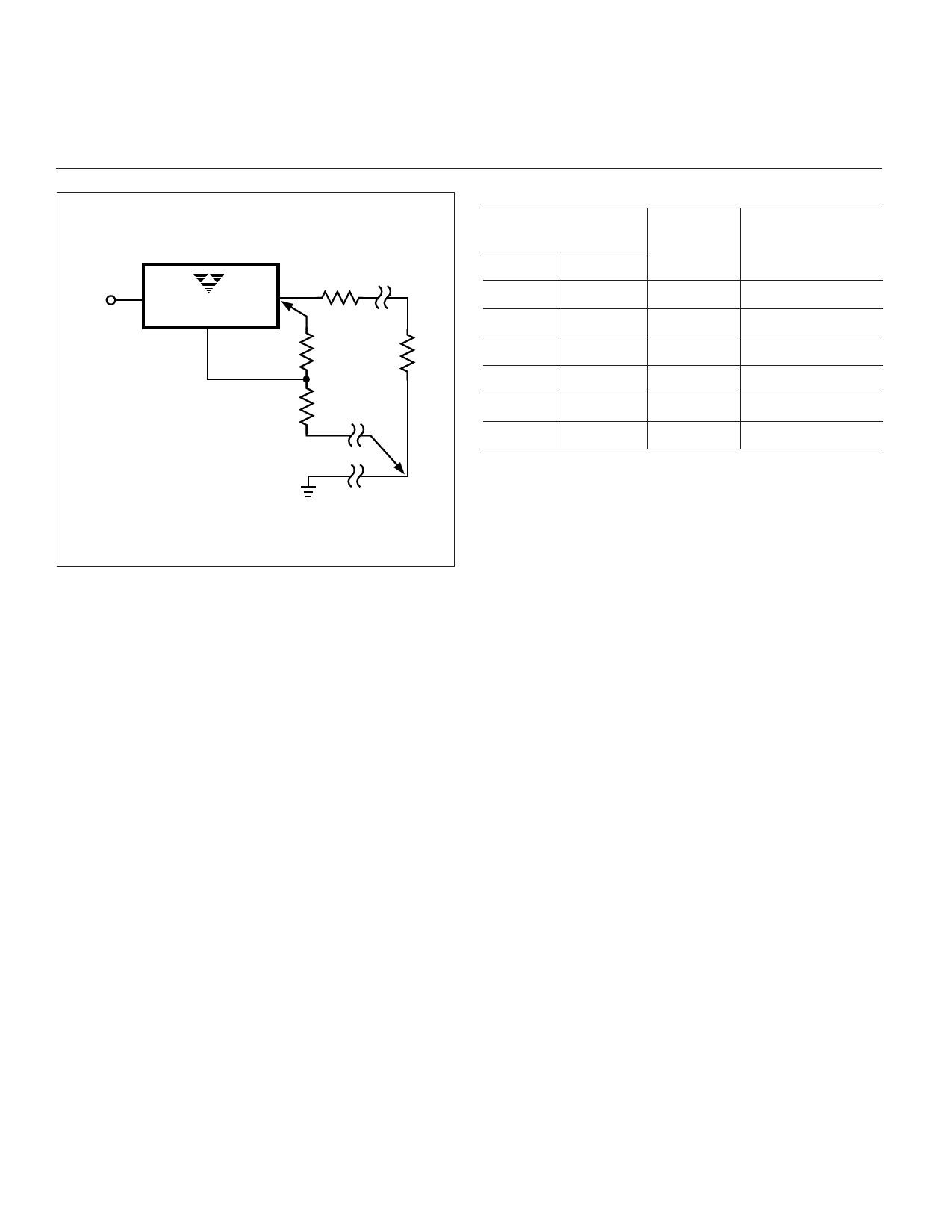
Rp
PARASITIC
LINE RESISTANCE
VIN
IN TCL1117 OUT
ADJ
R1
RL
CONNECT
R1 TO CASE
R2
Table 1.
Copper Area
Thermal
Resistance
Topside* Backside Board Area (Junction-to-Ambient)
2500 Sq. mm 2500 Sq. mm 2500 Sq. mm
45°C/W
1000 Sq. mm 2500 Sq. mm 2500 Sq. mm
45°C/W
225 Sq. mm 2500 Sq. mm 2500 Sq. mm
53°C/W
100 Sq. mm 2500 Sq. mm 2500 Sq. mm
59°C/W
1000 Sq. mm 1000 Sq. mm 1000 Sq. mm
52°C/W
1000 Sq. mm 0
1000 Sq. mm
55°C/W
*Tab of device attached to topside copper
CONNECT
R2 TO LOAD
Figure 3. Connections for Best Load Regulation
Power Dissipation and Thermal Design
As mentioned earlier, the TCL1117 has thermal over-
load protection which limits internal temperature to +165°C.
However, device functionality is only guaranteed to a maxi-
mum junction temperature of +125°C. Since internal power
dissipation can be >1 watt, careful thermal design is essen-
tial. The TCL1117 is supplied in a SOT-223 package which
is intended to be directly surface-mounted to the PC-board.
Because there is no dedicated heat sink, power dissipation
to ambient is performed largely by the PC board and its
copper material.
The power dissipation and junction temperature for the
TCL1117 in a SOT-223 are given by the following equations:
PD = (VIN – VOUT) x (IOUT)
TJUNCTION = TAMBIENT + (PD x ΘJA)
NOTE: TJUNCTION must not exceed 125°C
Soldering Methods
The recommended methods of soldering the SOT-223
package are: vapor phase re-flow and infrared re-flow with
component preheat within 65°C of the solder temperature.
Hand soldering and wave soldering methods are not recom-
mended since they can damage the part with excessive
thermal gradients across the surface area of the package.
Thermal shock to the package (>30°C per second) must be
minimized.
Ripple Rejection
Ripple Rejection curves were generated using an ad-
justable output TCL1117 with a bypass capacitor from ADJ
to ground. To obtain the performance shown in the curves,
the impedance of the bypass capacitor (at the ripple fre-
quency) should be less than R1. R1 is typically 100Ω to
200Ω. For example at 120Hz, with R1 = 100Ω, the adjust
capacitor should be at least 13µF. Only 0.16µF would be
required at 10kHz.
The output ripple increases as the ratio of the output
voltage to the reference voltage (VOUT/VREF) in fixed voltage
devices, and adjustable devices without an adjust pin ca-
pacitor. For example, at 5V, output ripple will increase by a
factor of 4 (5/1.25V). Ripple rejection will be reduced by 12db
from the value shown on the curve.
The ΘJC (junction to external tab) for the SOT-223 is
15°C/W. Depending upon heatsink parameters, the ΘCA can
be as low as 30°C/W. Therefore, the total thermal resistance
(ΘJA) is at least 45°C/W. Table 1 shows thermal resistance
measurements taken with the TCL1117 mounted on 1/16
inch 2-layer PCB with 1oz. copper foil. NOTE: The TAB pin
does not have to be soldered to all copper layers for effective
heat transfer. Use Table 1 only as a rough guide since
thermal interactions with adjacent components cannot be
predicted.
TCL1117-05 6/5/97
4
Share Link: