TA2020-020 Ver la hoja de datos (PDF) - Tripath Technology Inc.
Número de pieza
componentes Descripción
Fabricante
TA2020-020
Tripath Technology Inc.

TA2020-020 Datasheet PDF : 13 Pages
| |||
TECHNICAL INFORMATION
B
Pin Description
Pin
2, 8
3, 7,
16
4
6
9, 12
10, 13
11
Function
V5D, V5A
AGND1, AGND2,
AGND3
REF
OVERLOADB
VP1, VP2
IN1, IN2
MUTE
14
17
18
19, 28
20
21, 23,
26, 24
22, 25
1, 5, 15
27
29
30
31, 32
BIASCAP
SLEEP
FAULT
PGND2, PGND1
DGND
OUTP2 & OUTM2;
OUTP1 & OUTM1
VDD2, VDD1
NC
VDDA
CPUMP
5VGEN
DCAP2, DCAP1
Digital 5VDC, Analog 5VDC
Analog Ground
Description
Internal reference voltage; approximately 1.0VDC
A logic low output indicates the input signal has overloaded the amplifier.
Input stage output pins
Single-ended inputs. Inputs are a “virtual” ground of an inverting opamp with
approximately 2.4VDC bias.
When set to logic high, both amplifiers are muted and in idle mode. When low
(grounded), both amplifiers are fully operational. If left floating, the device stays in
the mute mode. Ground if not used.
Input stage bias voltage (approximately 2.4VDC).
When set to logic high, device goes into low power mode. If not used this pin
should be grounded.
A logic high output indicates thermal overload, or an output is shorted to ground,
or another output.
Power Ground (high current)
Digital Ground
Bridged outputs
Supply pin for high current H-bridges, nominally 13.5VDC.
Not connected
Analog 13.5VDC
Charge pump output (nominally 10V above VDDA)
Regulated 5VDC source used to supply power to the input section (pins 2 & 8).
Charge pump switching pins. DCAP1 (pin 32) is a free running 300kHz square
wave between VDDA and DGND (13.5Vpp nominal). DCAP2 (pin 31) is level
shifted 10 volts above DCAP1 (pin 32) with the same amplitude (13.5Vpp
nominal), frequency, and phase as DCAP1.
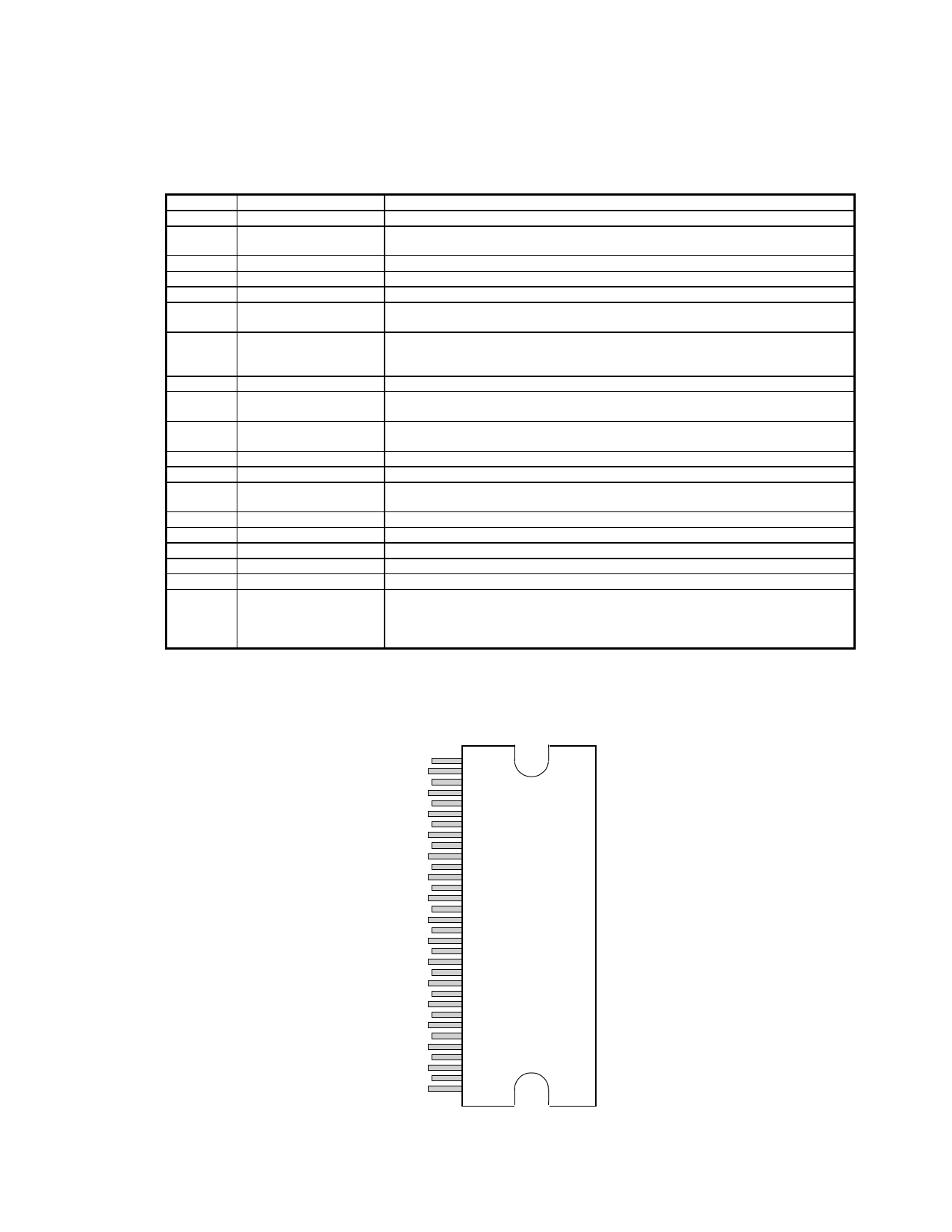
32-pin SSIP Package
(Front View)
NC
1
V5D
2
AGND1
3
REF
4
NC
5
OVERLOADB
6
AGND2
7
V5A
8
VP1
9
IN1
10
MUTE
11
VP2
12
IN2
13
BIASCAP
14
NC
15
AGND3
16
SLEEP
17
FAULT
18
PGND2
19
DGND
20
OUTP2
21
VDD2
22
OUTM2
23
OUTM1
24
VDD1
25
OUTP1
26
VDDA
27
PGND1
28
CPUMP
29
5VGEN
30
DCAP2
31
DCAP1
32
4 of 13
TA2020-020, Rev. 4.0, 09.00
Share Link: