TA1101B Ver la hoja de datos (PDF) - Tripath Technology Inc.
Número de pieza
componentes Descripción
Fabricante
TA1101B
Tripath Technology Inc.

TA1101B Datasheet PDF : 13 Pages
| |||
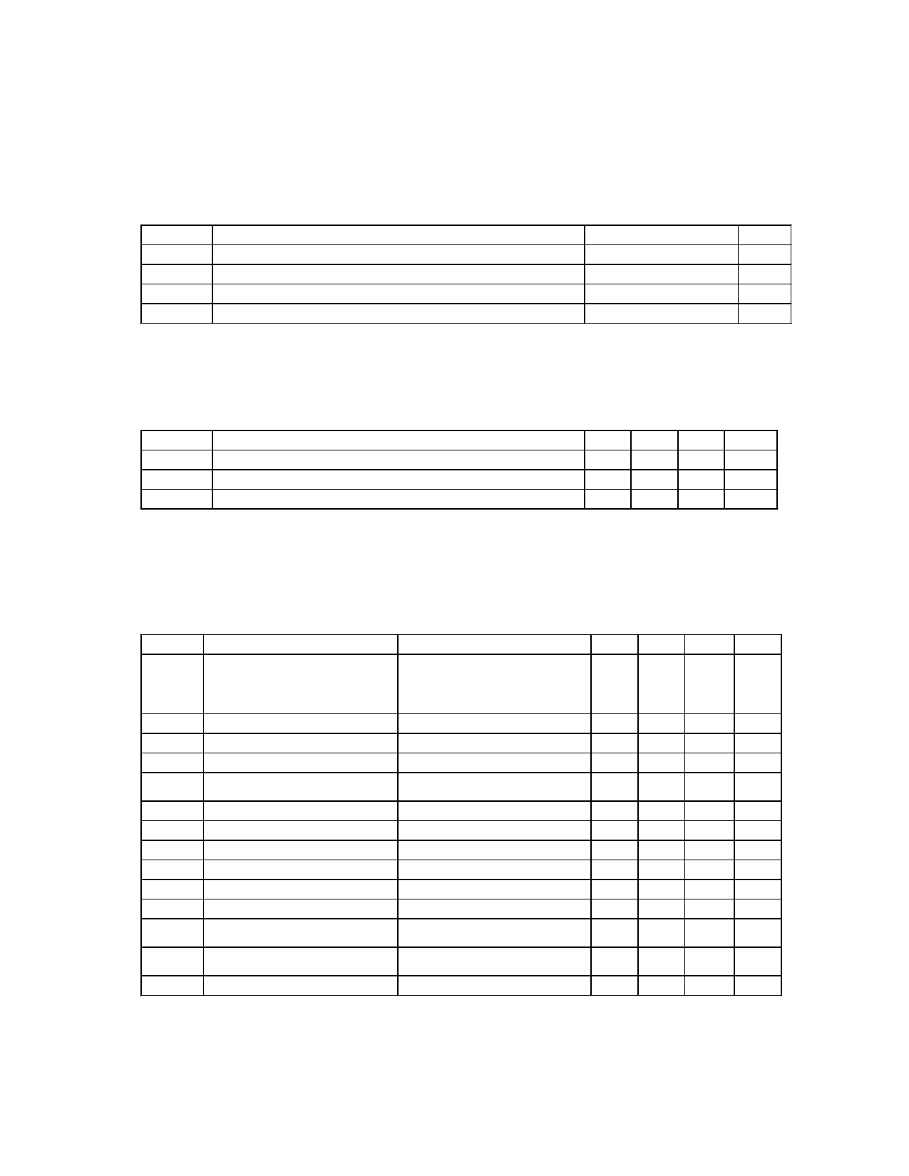
TECHNICAL INFORMATION
Absolute Maximum Ratings (Note 1)
SYMBOL
VDD
TSTORE
TA
PDISS
PARAMETER
Supply Voltage
Storage Temperature Range
Operating Free-air Temperature Range
Continuous Total Power Dissipation
Value
16
-40° to 150°
0° to 70°
Note 2
UNITS
V
C
C
W
Note 1: Absolute Maximum Ratings indicate limits beyond which damage to the device may occur.
Note 2: See Power Dissipation Derating in the Applications Information section.
Operating Conditions (Note 3)
SYMBOL
VDD
VIH
VIL
PARAMETER
Supply Voltage
High-level Input Voltage (MUTE, SLEEP)
Low-level Input Voltage (MUTE, SLEEP)
MIN.
8.5
3.5
TYP.
12
MAX.
13.2
1
UNITS
V
V
V
Note 3: Recommended Operating Conditions indicate conditions for which the device is functional. See
Electrical Characteristics for guaranteed specific performance limits.
Electrical Characteristics
See Test/Application Circuit. Unless otherwise specified, VDD = 12V, f = 1kHz, Measurement
Bandwidth = 22kHz, RL = 4Ω, TA = 25 °C, Package heat slug soldered to 2.8 square-inch PC pad.
SYMBOL
PARAMETER
CONDITIONS
MIN. TYP. MAX. UNITS
PO
Output Power
(Continuous Average/Channel)
IDD,MUTE Mute Supply Current
THD+N = 0.1%
THD+N = 10%
MUTE = VIH
RL = 4Ω
RL = 8Ω
RL = 4Ω
RL = 8Ω
9
11
W
5.5
6
W
12
16
W
8
10
W
5.5
7
mA
IDD, SLEEP Sleep Supply Current
SLEEP = VIH
0.25
2
mA
Iq
Quiescent Current
VIN = 0 V
61
75
mA
THD + N Total Harmonic Distortion Plus
Noise
IHF-IM IHF Intermodulation Distortion
PO = 9W/Channel
19kHz, 20kHz, 1:1 (IHF)
0.04
%
0.18 0.5
%
SNR
Signal-to-Noise Ratio
A-Weighted, POUT = 1W, RL = 8Ω
89
dB
CS
Channel Separation
30kHz Bandwidth
50
55
dB
PSRR Power Supply Rejection Ratio
Vripple = 100mV.
60
80
dB
η
Power Efficiency
POUT = 10W/Channel, RL = 8Ω
88
%
VOFFSET Output Offset Voltage
No Load, MUTE = Logic Low
50
150
mV
VOH
VOL
eOUT
High-level output voltage
(FAULT & OVERLOAD)
Low-level output voltage
(FAULT & OVERLOAD)
Output Noise Voltage
3.5
V
1
V
A-Weighted, input AC grounded
100
µV
Note: Minimum and maximum limits are guaranteed but may not be 100% tested.
2
TA1101B, Rev. 2.2, 08.17.00
Share Link: