TA1101B Ver la hoja de datos (PDF) - Tripath Technology Inc.
Número de pieza
componentes Descripción
Fabricante
TA1101B
Tripath Technology Inc.

TA1101B Datasheet PDF : 13 Pages
| |||
TECHNICAL INFORMATION
Sleep Pin
The SLEEP pin is a 5V logic input that when pulled high (>3.5V) puts the part into a low quiescent current
mode. This pin is internally clamped by a zener diode to approximately 6V thus allowing the pin to be
pulled up through a large valued resistor (1MΩ recommended) to VDD. To disable SLEEP mode, the sleep
pin should be grounded.
Fault Pin
The FAULT pin is a 5V logic output that indicates various fault conditions within the device. These
conditions include: low supply voltage, low charge pump voltage, low 5V regulator voltage, over current at
any output, and junction temperature greater than approximately 155°C. All faults except overcurrent all
reset upon removal of the condition. The FAULT output is capable of directly driving an LED through a
series 200Ω resistor. If the FAULT pin is connected directly to the MUTE input an automatic reset will
occur in the event of an over-current condition.
Power Dissipation Derating
For operating at ambient temperatures above 25°C the device must be derated based on a 150°C
maximum junction temperature, TJMAX as given by the following equation:
PDISS
=
(TJMAX − TA )
θJA
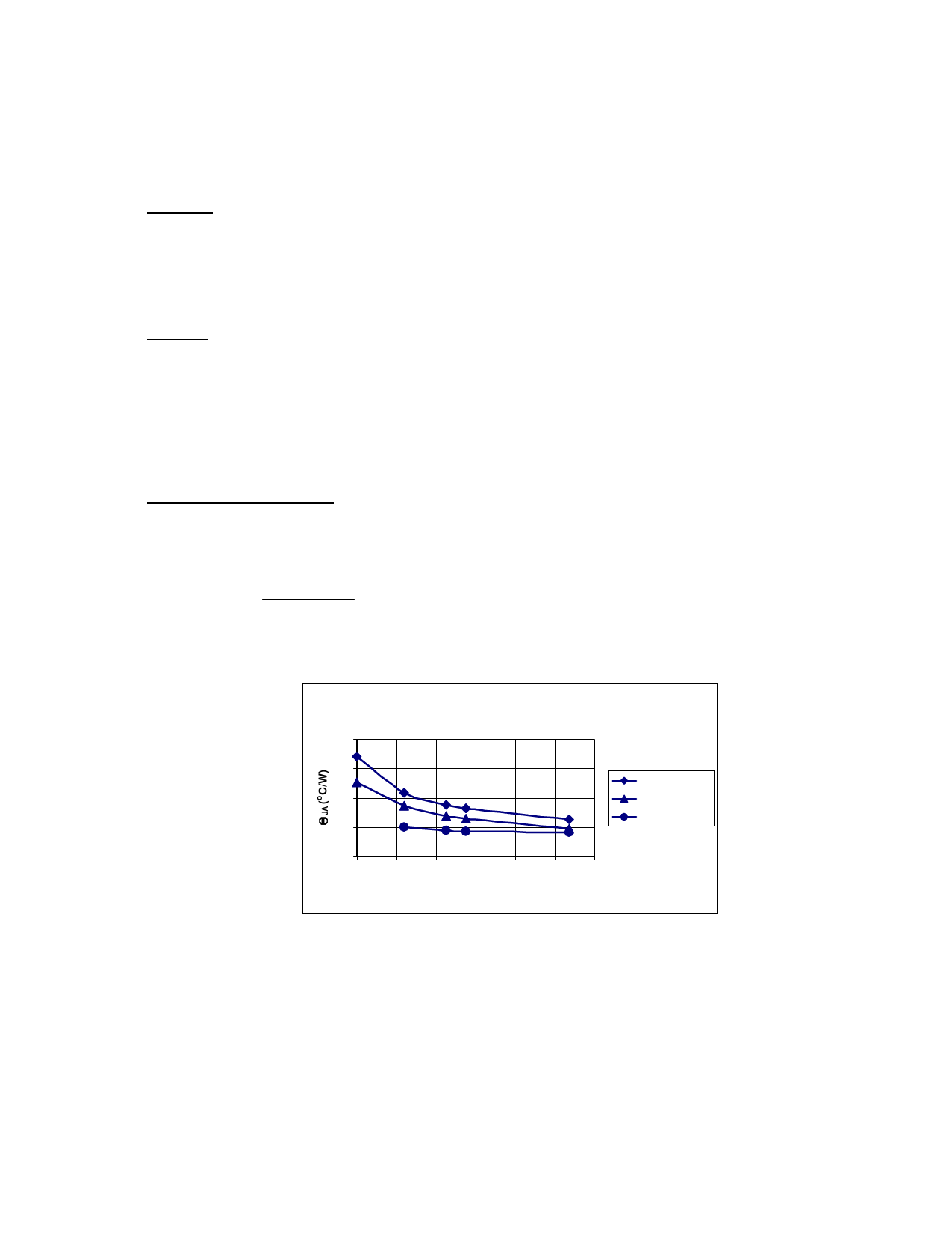
Where θJA of the package is determined from the following graph:
50
40
30
20
10
0
Θ JA vs Copper Area
1
2
3
4
5
6
Copper Area (square inches)
Pdiss - 1.35W
Pdiss - 2W
Pdiss - 3.4W
In the above graph Copper Area is the size of the copper pad on the PC board to which the heat slug of
the TA1101B is soldered. The heat slug must be soldered to the PCB to increase the maximum power
dissipation capability of the TA1101B package. Soldering will minimize the likelihood of an over-
temperature fault occurring during continuous heavy load conditions. The vias used for connecting the
heatslug to the copper area on the PCB should be 0.013” diameter.
10
TA1101B, Rev. 2.2, 08.17.00
Share Link: