PF28F1602C3TD70 Ver la hoja de datos (PDF) - Intel
NГәmero de pieza
componentes DescripciГіn
Fabricante
PF28F1602C3TD70 Datasheet PDF : 75 Pages
| |||
C3 SCSP Flash Memory
1.4
Signal Definitions
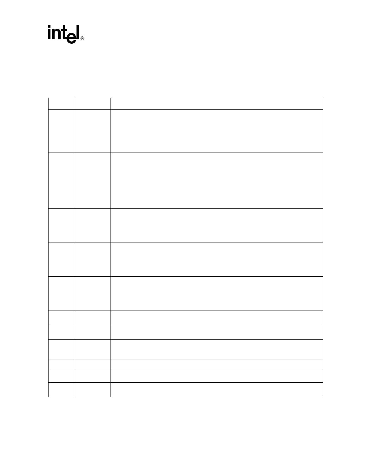
Table 2.
Symbol
A[20:0]
DQ[15:0]
F-CE#
S-CS1#
S-CS2
F-OE#
S-OE#
F-WE#
S-WE#
S-UB#
S-LB#
Table 2 defines the signals shown in Figure 1 вҖң66-Ball SCSP Package BalloutвҖқ on page 8.
IntelВ® Advanced+ Boot Block SCSP Ball Descriptions (Sheet 1 of 2)
Type
INPUT
INPUT /
OUTPUT
INPUT
INPUT
INPUT
INPUT
INPUT
INPUT
INPUT
INPUT
INPUT
Name and Function
ADDRESS INPUTS for memory addresses. Addresses are internally latched during a program or
erase cycle.
вҖў 2-Mbit : A[16:0]
вҖў 4-Mbit : A[18:0]
вҖў 16-Mbit : A[19:0]
вҖў 32-Mbit A[20:0]
DATA INPUTS/OUTPUTS:
вҖў Inputs array data for SRAM write operations and on the second F-CE# and F-WE# cycle
during a flash program command.
вҖў Inputs commands to the flash memory Command User Interface when F-CE# and F-WE# are
asserted.
вҖў Data is internally latched.
вҖў Outputs array, configuration, and status register data.
The data balls float to tristate when the chip is deselected or the outputs are disabled.
FLASH CHIP ENABLE: Activates the flash internal control logic, input buffers, decoders, and
sense amplifiers.
вҖў F-CE# is active low.
вҖў F-CE# high deselects the flash memory device and reduces power consumption to standby
levels.
SRAM CHIP SELECT1: Activates the SRAM internal control logic, input buffers, decoders, and
sense amplifiers.
вҖў S-CS1# is active low.
вҖў S-CS1# high deselects the SRAM memory device and reduces power consumption to standby
levels.
SRAM CHIP SELECT2: Activates the SRAM internal control logic, input buffers, decoders, and
sense amplifiers.
вҖў S-CS2 is active high.
вҖў S-CS2 low deselects the SRAM memory device and reduces power consumption to standby
levels.
FLASH OUTPUT ENABLE: Enables flash memory outputs through the data buffers during a read
operation. F-OE# is active low.
SRAM OUTPUT ENABLE: Enables SRAM outputs through the data buffers during a read
operation. S-OE# is active low.
FLASH WRITE ENABLE: Controls writes to the flash memory command register and memory
array. F-WE# is active low. Addresses and data are latched on the rising edge of the second
F-WE# pulse.
SRAM WRITE ENABLE: Controls writes to the SRAM memory array. S-WE# is active low.
SRAM UPPER BYTE ENABLE: Enables the upper byte for SRAM (DQ8вҖ“DQ15).
S-UB# is active low.
SRAM LOWER BYTE ENABLE: Enables the lower byte for SRAM (DQ0вҖ“DQ7).
S-LB# is active low.
Datasheet
IntelВ® Advanced+ Boot Block Flash Memory (C3) SCSP Family
Order Number: 252636, Revision: 004
26 Aug 2005
9
Share Link: 