28F016XS Ver la hoja de datos (PDF) - Intel
Número de pieza
componentes Descripción
Fabricante
28F016XS Datasheet PDF : 54 Pages
| |||
28F016XS FLASH MEMORY
E
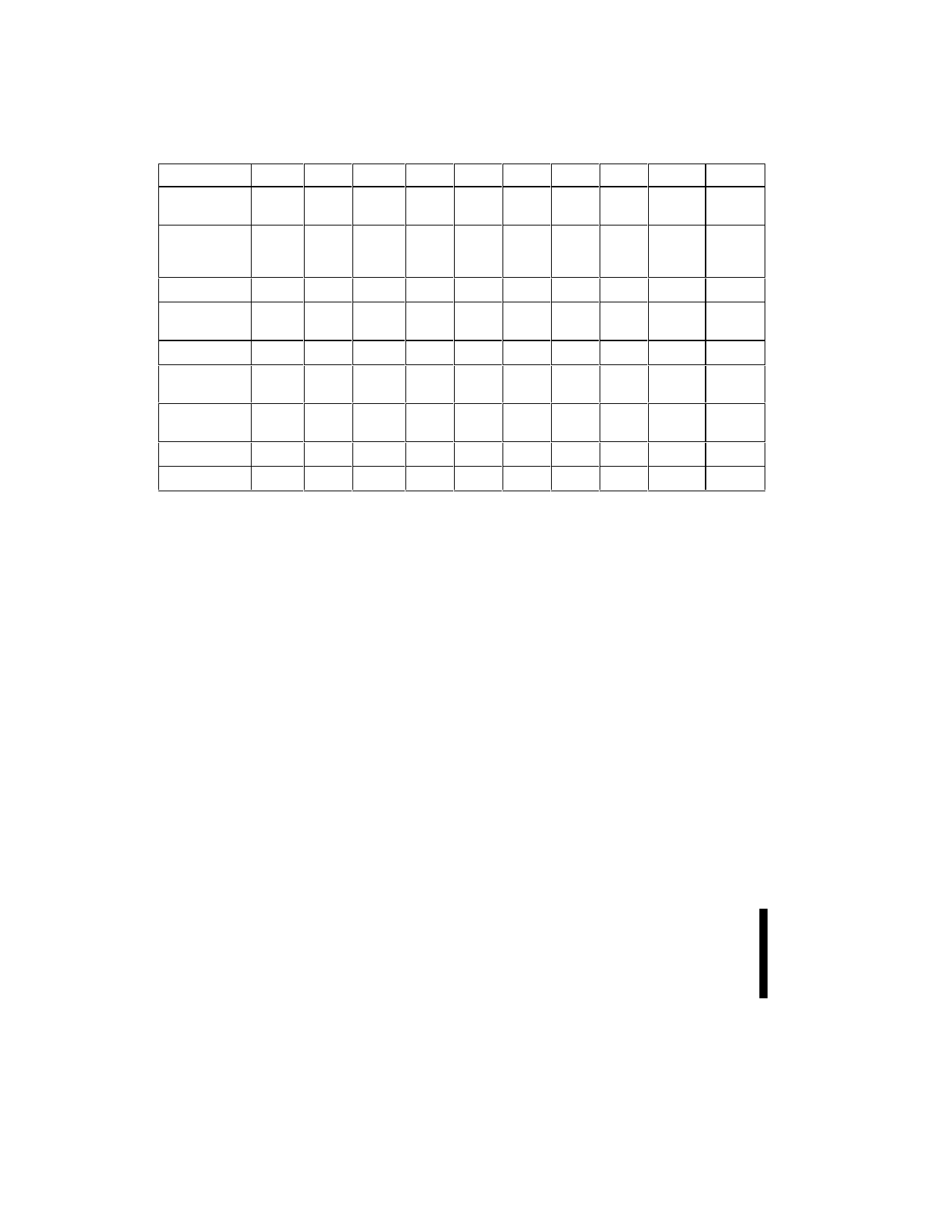
4.0 BUS OPERATIONS, COMMANDS AND STATUS REGISTER DEFINITIONS
4.1 Bus Operations for Word-Wide Mode (BYTE# = VIH)
Mode
Latch Read
Address
Notes RP# CE0–1# OE# WE# ADV# CLK A1 DQ0–15 RY/BY#
1,9,10 VIH
VIL
X
VIH
VIL
↑
X
X
X
Inhibit
Latching
1,9
VIH
VIL
X
VIH
VIH
↑
X
X
X
Read Address
Read
Output
Disable
1,2,7,9 VIH
VIL
VIL
VIH
X
↑
X
DOUT
X
1,6,7,9 VIH
VIL
VIH
VIH
X
X
X High Z
X
Standby
1,6,7,9 VIH
VIL
X
X
X
X
X High Z
X
Deep
1,3
VIL
X
X
X
X
X
X
High Z
VOH
Power-Down
Manufacturer 1,4,9 VIH
VIL
VIL
VIH
X
ID
↑
VIL 0089H
VOH
Device ID
1,4,8,9 VIH
VIL
VIL
VIH
X
↑
VIH 66A8H
VOH
Write
1,5,6,9 VIH
VIL
VIH
VIL
X
X
X
DIN
X
NOTES:
1. X can be VIH or VIL for address or control pins except for RY/BY#, which is either VOL or VOH, or High Z or DOUT for data
pins depending on whether or not OE# is active.
2. RY/BY# output is open drain. When the WSM is ready, Erase is suspended, or the device is in deep power-down mode,
RY/BY# will be at VOH if it is tied to VCC through a resistor. RY/BY# at VOH is independent of OE# while a WSM operation
is in progress.
3. RP# at GND ± 0.2V ensures the lowest deep power-down current.
4. A0 and A1 at VIL provide device manufacturer codes in x8 and x16 modes respectively. A0 and A1 at VIH provide device ID
codes in x8 and x16 modes respectively. All other addresses are set to zero.
5. Commands for erase, data program, or lock-block operations can only be completed successfully when VPP = VPPH1 or
VPP = VPPH2.
6. While the WSM is running, RY/BY# stays at VOL until all operations are complete. RY/BY# goes to VOH when the WSM is
not busy or in erase suspend mode.
7. RY/BY# may be at VOL while the WSM is busy performing various operations (for example, a Status Register read during a
write operation).
8. The 28F016XS shares an identical device identifier with the 28F016XD.
9. CE0–1# at VIL is defined as both CE0# and CE1# low, and CE0–1# at VIH is defined as either CE0# or CE1# high.
10. Addresses are latched on the rising edge of CLK in conjunction with ADV# low. Address A1 = 0 selects the even bank and
A1 = 1 selects the odd bank, in both byte-wide mode and word-wide mode device configurations.
16
Share Link: 