AN-6846 Ver la hoja de datos (PDF) - Fairchild Semiconductor
Número de pieza
componentes Descripción
Fabricante
AN-6846
Fairchild Semiconductor

AN-6846 Datasheet PDF : 8 Pages
| |||
AN-6846
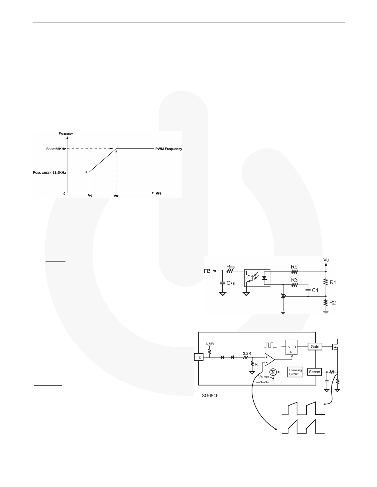
The proprietary green mode provides off-time modulation to
reduce the PWM frequency at light-load and no-load
conditions. The feedback voltage of the FB pin is taken as a
reference. As shown in Figure 7, when the feedback voltage
is lower than about 2.1V, the PWM frequency decreases.
Because most losses in a switching-mode power supply are
proportional to the PWM frequency, the off-time modulation
reduces the power consumption of the power supply at light-
load and no-load conditions. For a typical case of RI=26KΩ,
the PWM frequency is 65kHz at nominal load and decreases
to 22.5kHz at light loads, about one third of the nominal
PWM frequency. The power supply enters burst mode at
zero-load conditions.
Figure 7. PWM Frequency vs. FB Voltage
FB Input
The SG6846 is designed for peak-current-mode control. A
current-to-voltage conversion is accomplished externally
with current-sense resistor RS. Under normal operation, the
FB level controls the peak inductor current:
I pk
=
VFB − 1.2
4.2 ⋅ RS
(4)
where VFB is the voltage of FB pin.
When VFB is less than 1.6V, the SG6846 terminates the
output pulses.
APPLICATION NOTE
Built-in Slope Compensation
A flyback converter can be operated in discontinuous
current mode (DCM) or continuous current mode (CCM).
With the same output power, a converter in CCM exhibits
smaller peak inductor current than in DCM. Therefore, a
small-sized transformer and a low-rating MOSFET can be
applied. On the secondary side of the transformer, the rms
output current of DCM can be up to twice that of CCM.
Larger wire gauge and output capacitors with larger ripple
current ratings are required. DCM operation also results in
higher output voltage spikes. A large LC filter has to be
added. Therefore, a flyback converter in CCM achieves
better performance with lower component cost.
Despite the above advantages of CCM operation, there is
one concern – stability. In CCM operation, the output power
is proportional to the average inductor current, while the
peak current is controlled. This causes the well-known sub-
harmonic oscillation when the PWM duty cycle exceeds
50%. Adding slope compensation (reducing the current-loop
gain) is an effective way to prevent oscillation. The SG6846
introduces a synchronized positive-going ramp (VSLOPE) in
every switching cycle to stabilize the current loop.
Therefore, the SG6846 enables design of a cost-effective,
highly efficient, compact flyback power supply operating in
CCM without adding external components.
The positive ramp added is:
VSLOPE = VSL ⋅ D
(6)
0 is a typical feedback circuit mainly consisting of a shunt
regulator and an opto-coupler. R1 and R2 form a voltage
divider for output voltage regulation. R3 and C1 are
adjusted for control-loop compensation. A small-value RC
filter (e.g. RFB= 47Ω, CFB= 1nF) placed from the FB pin to
GND can increase stability substantially. The maximum
source current of the FB pin is about 2mA. The
phototransistor must be capable of sinking this current to
pull the FB level down at no load. The value of the biasing
resistor, Rb, is determined as:
Vo − VD −VZ ⋅ K ≥ 2mA
Rb
(5)
where:
VD is the drop voltage of photodiode, about 1.2V;
VZ is the minimum operating voltage, 2.5V of the shunt
regulator; and
K is the current transfer rate (CTR) of the opto-coupler.
For an output voltage VO=5V, with CTR=100%, the
maximum value of Rb is 650Ω.
Figure 8. Feedback Circuit
where VSL = 0.33V and D = duty cycle.
Figure 9. Synchronized Slope Compensation
© 2008 Fairchild Semiconductor Corporation
Rev. 1.3.2 • 9/26/08
4
www.fairchildsemi.com
Share Link: